
|
| |
|
Строительный блокнот Introduction to electronics lator system. The compensator network is designed to attain adequate pliase margin and good rejection of expected disturbances. Lead compensators and P-D controllers are used to improve the phase margin and extend the bandwidth of the feedback loop. This leads to better rejection of high-frequency disturbances. Lag compensators and P-I controllers are used to increase the low-frequency loop gain. This leads to better rejection of low-frequency disturbances and very small steady-state error. More complicated compensators can achieve the advantages of both approaches. Injection methods for experimental measurement of loop gain are introduced in Section 9.6. The use of voltage or current injection solves the problem of establishing the correct quiescent operating point in high-gain systems. Conditions forobtaining an accurate measurement are exposed. The injection method also allows measurement of the loop gains of unstable systetns. 9.2 EFFECT OF NEGATIVE FEEDBACK ON THE NETWORK TRANSFER FUNCTIONS We have seen how to derive the small-signal ac transfer functions of a switching converter. For example, the equivalent circuit model of the buck converter can be written as in Fig. 9.3. This equivalent circuit Contains three independent inputs: the control input variations d. the power input voltage variations P and the load current variations The output voltage variation V can therefore be expressed as a linear combination of the three independent inputs, as follows: v{s)G, where d(.s) convertet conlrol-to-outpul transfer function (y.lii) if ill converter line-to-output transfer function (9.1b) convener output impedance (9.lL) The Bode diagrams of these quantities are constructed in Chapter 8. Equation (9.1) describes how distur- Q-, ,-ПЛПГ 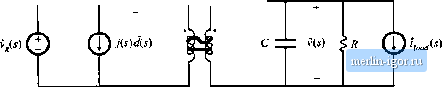 Fig, 93 Smitll-signal converter inodel, which rcpitisents variations in d, and 9.2 Effect nf Negative Feedltcick on tlie Netw/orli Ттпфг Functions 335 bantes and Jj, y propagate to the output v, through the transfer funetion G.(y} and the output imped-anee Z i{s)- If the distuibanees and if j are known to have some maximum worst-ease amplitude, then Eq. (9.1) tan be used to compute the resulting worst-case open-loop variation in v. As de.scribed previously, the feedback loop of Fig. 9.2 can be used to reduce the influences of v, and ( j on the output v. To analyze this system, let us perturb and linearize its averaged signals about their quiescent operating points. Both the power stage and the control block diagram are perturbed and linearized: v,(O = V, + 0/) etc. In a dc regulator system, the reference input is constant, so v,p) - 0. In a switching amplifier or dc-ac inverter, the reference input may contain an ac variation. In Fig. 9.4(a). the converter model of Fig. 9.3 is combined with the petturbed and linearized control circuit block diagram. This is equivalent to the reduced block diagram of Fig. 9.4(b). in which the converter model has been replaced by blocks representing Eq. (9.1). Solution of Fig. 9.4(b) for the output voltage variation v yields G,G,yVV . Z, (9.3) which can be written in the form -/H 1 + r 1 -t-r 1 -t-r with Г{1) = W(j)G (i)G /.i)/V = loop gain Equation (9.4) is a getieral result. The loop gain TTi) is defined iti general as the product of the gains around the forward and feedback paths of the loop. This equation .shows how the addition of a feedback loop modifies the transfer functions and performance ofthe system, as described in detail below. 9.2.1 FEEdback Reduces the Transfer Functions firORt Disturbances to the Output The transfer function from v, to v in the opeti-loop buck conveiter of Fig. 9.3 is G.X ). as given in Eq. (9.1). When feedback is added, this transfer function becomes v (.v) c,.ns) from Eq. (9.4), So this transfer function is reduced via feedback by the factor 1/(1 4 T{i)). If the loop gain r(.t)is large in magnitude, then the reduction can be substantial. Hence, the output voltage variation i> resulting from agiven v, variation is attenuated by the feedback loop. 1; M(D) ТЛПГ 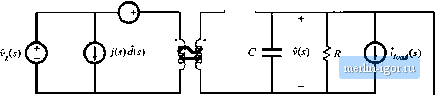 Reference input
Hums) Pulse-width modulator His) Sensor gain Reference input Compensator ac tine variation Pulse-wldtb modulator Error signal
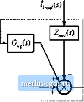 Load current variation vis) variation ------------- Converter power stage Output voitage variation Hisms) His) Sensor gain ¥ig. 9Л Voltage regulator system stnall-sjgrial model: (a) with converter equivalent circuit; (b) complete block diagram. |
|||||||||||||||||||||||||||