
|
| |
|
Строительный блокнот Introduction to electronics Maximum piiase lead Fig. 9.16 Maximum phase lead 9 vs. frequency ratio j for Ihe lead compensator, 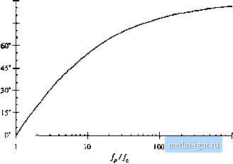 1000 extended while maintaining an acceptable phase margin. A side effect ofthe zero is that it causes the compensator gain to increase with frequency, with a +20 dB/decade slope. So steps must be talten to ensure that ! T\\ remains equal to unity at the desired crossover frequency. Also, since the gain of any practical amplifier must tend to zero at high frequency, the compensator transfer function G,.is) must contain high frequency poles. These poles also have the beneficial effect of attenuating high-frequency noise. Of particular concern are the switching frequency harmonics present in the output voltage and feedback signals. If the compensator gain at the switching frequency is too great, then these switching harmonics are amplified by the compensator, and can disrupt the operation ofthe pulse-width modulator (see Section 7.6). So the compensator network should contain poles at a frequency less than the switching frequency. These considerations typically restrict the crossover frequency /j, to be less than approximately MWi- ofthe converter swdching frequency f. In addition, the circuit designer must take care not to exceed the gain-bandwidth limits of available operational amplifiers. The transfer function of the lead compensator therefore contains a low-frequency zero and several high-frequency poles. A simplified example containing a single high-frequency pole is given in Eq. (9.32) and illustrated m Fig. 9.15. (9.32) The maximum phase occurs at a frequency f ,i given by the geometrical mean ofthe pole and zero frequencies: (9,33) To obtain the maximum improvement in phase margin, we should design our compensator so that the frequency coincides with the loop gain crossover frequency f.. The value ofthe phase at this frequency can be shown to be 60 dB 40 dB 20 dB OdB -20 dB 0 dB lirii Cnmpensaled gain yj ConYpcnsaied phase asympioies Driginiil phase asymploics 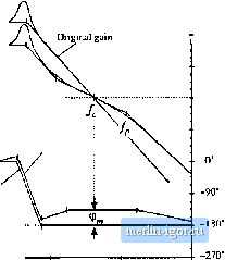 Fig. 9.17 Ctjmpeiisatinn tif a loop gain tionlainiiig two poles, using a lead (PD) compensator, ihe phase margin ф is improved. tJ,(/,)=tan- (9,34) This equation is plotted in Fig. 9.16, Equation (9.34) can be inverted to obtain £+sin0} Л l-sin(9) (9.35) where 9 =-С.(/, ). Equations (9.34) and (9.32) imply that, to optimally obtain a competisator phase lead of 6 at frequency/j., the pole and zero frequencies should be chosen as follows: f, = i- 1 -sin(e) 1 + sin(ej I + sin (6) 1 - sin (ej (.36) When it is desired to avoid changing the crossover frequency, the magnitude of the compensator gain is chosen to be unity at the loop gain crossover frequency /,. This requires that G be chosen according to the following formula: (9,37) h can be seen that С.д is less than unity, and therefore the lead compensator reduces the dc gain of the feedback l(X)p. Other choices of f;,jCan be selectetl when it is desired to shift the crossover frequency f.; for exatnple, increasing the value of causes the crossover frequency to increase. If the frequencies and/j arc chosen as in Eq. (9,3fi), then .of Eq. (9.32) will coincide with the new crossover frequency The Bode diagratn of a typical loop gain T{s) containing two poles is illustrated in Fig. 9.17. The phase margin of the original 7(.т) is small, since the crossover frequency is.substantiallygreater than the pole frequency /9. The result of adding a lead compensator is al.so illustrated. The lead compensator of this example is designed to maintain the siime crossover fre(]uency but improve the phiLse mat-gin. 9.5.2 Lag (PT) Compensatur This type of cotnpensator is used to increase the low-frequency loop gain, such that the output is better regulated at dc and at frequencies well below the loop crossover frequency. As given in Eq. (9.38) and illustrated in Fig. 9.18, an inverted zero is added to the loop gain, atfrequency/j. (9.38) Uf is sufficiently lower than the loop crossover frequency f., then the phase tnargin is unchanged. This type of compensator is iilso tiilled a.pmporlional-plu.i-mtegral, ot PI, controller-at low frequencies, the inverted zero tau.4es the cinnpensator to integrate the etror signal. To the extent thatthecompeusator gain tan be tnade arbitrarily large atdc, the dc loop gain 7i[0) becomes arbitrarily large. This causes the dc cotnponent ofthe error signal to approach zero. In consequence, the steady-state output voltage is perfectly regulated, and the disturbance-to-output transfer functions approach zero at dc. Such behavior is easily obtained in practice, with the cotnpetisator of Et], (9.38)realized using aconventional operational atnplifier. Although the PI cotnpensator is useful in tiearly all types of feedback systems, it is an especially sitnple and effective approach for sy.stems originally containing a single pole. For the example of Fig. 9.19, theoriginal uticotnpensated loop gain is ofthe fortn Fig. 9,IS Magnitude and phase asymptotes of die P! compensator transfer function G. of Eq.(9.38).
|