
|
| |
Строительный блокнот Introduction to electronics 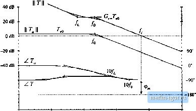 i 11: 10 Hz 100 Hi IkHi 100 kHz Fig. 9.19 Compeiibation nf a loop gain containing a single pole, using a kig (Pf) compensator. The loop gain magnitude is incicased. (9.39) The compensator transfer function t)f Eq. (9.38) is used, so that the compensated lt)op gain is T(s)-TJs)GJ,s:). Magnitude and phase asymptotes of T(.\) are also illushated in Fig. 9.19. The compensator high-frequency gain G is chosen to ohtain the desired crossover frequency /.. If we approximate the compensated loop gain hy its high-frequency asymptote, then at high frequencies we can write (9.40) At the crossover frequency/ = /., the loop gain has unity magnitude. Equation (9.40) predicts that the crossover frequency is (9.4!) Hence, to obtain a desired crossover frequency /., we should choose the compensator gain as follows: (9,42) The corner frequency Д is then cho.sen to he sufficiently less than such that an adequate phase margin ismaintained. IVlagnitude asymptotes of the quantity 1,(1 + T{s)) are constructed in Fig. 9.20. At frequencies 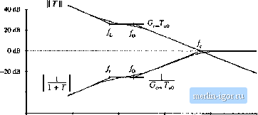 -40 dB I Hz 10 Hz 100 Hz IkHz 10 kHz 100kHz Mg. 9.20 Cniistruction nf II 1/(1 + 7) for tlie i/.tompeiisuted oxamjile of Ilg, 9.19, less than the Weorapensator improves the rejeetion ofdistiirbances. Aide, where the magnitude of G. approaches infinity, the magnitude of 1/(1 +7) tends to zero. Hence, the clt)sed-loop disturhanee-to-out-put transferfunctions, such as Eqs. (9.30) and (9.31), tend to zero atdc. 9.5.3 Combitted (PID) Compensator The advantages ofthe lead and lag compensators can be combined, to obtain both wide bandwidth and zero steady-state error. At low frequencies, the cotnpensator integrates the error signal, leading to large low-frequency loop gain and accurate regulation of the low-frequency components ofthe output voltage. At high frequency (in the vicinity ofthe crossover frequency), the compensator intrt)diices phase lead into the lt)op gain, improving the phase margin. Such a compensator is sometimes called a PID ctmtrol-ler. 40 dB 20 dB -20 dB -40 dB
0* -90* -180 Fisj. 9.21 Magnitude and phase asymptotes of ttie combined (P!D) compensator transfei funcdon G of Eq, (9,43). A typical Bode diagram ot a practical version of this compensator is illustrated in Fig. 9.21. The compensator has transfer function (4,43) The inverted zero at frequency j) functions in the same manner as the PI compensator. The zero at frequency/adds phase lead in the vicinity of the crossover frequency, as in the PD compensator. The high-frequency poles at frequencies and/J,j must be present in practical compensators, to cause the gain to roll off at high frequencies and to prevent the switching ripple from disrupting the operation of the pulse-width modulator. The loop gain crossover frequency is chosen to be greater than Д and , but less than fpi and/j,3. 9.5.4 Design Eicample To illustrate the design of W and PD compensators, let us consider the design of a combined PID compensator for the dc-dc buck converter system of Fig. 9.22. The input voltage vit) for this system has nominal value 28 V. li is desired to supply a regulated 15 V to a 5 A load. The load is modeled here with a 3 Й resistor. An accurate 5 V reference is available. The first step is to select the feedback gain H{s). The gain H is chosen such that the regulator produces a regulated 15 V dc output. Let us assume that we will succeed in designing a gMxi feedback system, which causes the output voltage to accurately follow the reference voltage. This is accomplished via a large loop gam T, which leads to a small error voltage: \\, ~ 0. Hence, Ilv ~ v.. So we should choose (Ч.44) The quiescent duty cycle is given by the steady-state solution of the converter: 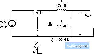 Transistor gate driver
Error signal Sensor gain Vj = 4 V Compensator Fig. 9.22 Desigu exainpic. |