Строительный блокнот  Introduction to electronics 

1 2 3 4 5 6 7 8 9 10 11 12 13 14 15 16 17 18 19 20 21 22 23 24 25 26 27 28 29 30 31 32 33 34 35 36 37 38 39 40 41 42 43 44 45 46 47 48 49 50 51 52 53 54 55 56 57 58 59 60 61 62 63 64 65 66 67 68 69 70 71 72 73 74 75 76 77 78 79 80 81 82 83 84 85 86 87 88 89 90 91 92 93 94 95 96 97 98 99 100 101 102 103 104 105 106 107 108 109 110 111 112 113 114 115 116 117 118 [ 119 ] 120 121 122 123 124 125 126 127 128 129 130 131 132 133 134 135 136 137 138 139 140 141 142 143 144 145 146 147 148 149 150 151 152 153 154 155 156 157 158 159 160 161 162 163 164 165 166 167 168 169 170 171 172 173 174 175 176 177 178 179 180 181 182 183 184 185 186 187 188 189 190 191 192 193 194 195 196 197 198 199 200 201 202 203 204 205 206 207 208 209 210 211 212 213 214 215 216 217 218 219 220 221 222 223 224 225 226 227 228 229 230 231 232 233 234 235 236 237 238 239 240 241 242 243 244 245 246 247 248 249 250 251 252 253 254 255 256 257 258 259 260 261 262 263 264 265 266 267 268 269 270 271 272 273 274 275 276 277 278 279 280 281 282 283 284 285 286 287 288 289 290 291 292 293 294 295 296 297 298 299 300


Error signal

) *

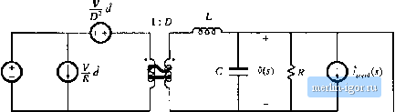
Compensator

His) 4s)

1m = 4V

Fig, 9.23 System small-signal яс model, design example.

Tis)

v.. 2

f9.45)

Tlie quiescent value ofthe control vtdtage, V, must satisfy Eq. (7.173). Hence,

V, = DV =2.14 V

(9.46)

Thtis, the quiescent conditions ofthe system are known. It remains to design the compensatorgain G{s).

A small-signal ac model ofthe regulator system is illustrated in Fig. 9.23. The buck converter ac model is represented in canonical form. Disturhances in the input voltage and in the load current are modeled. For generality, reference voltage variations are included in the diagram; in a dc voltage regulator, these variations are normally zero.

The t)pen-loop converter transfer functions are discussed in the previous chapters. The open-loop control-to-output transfer function is

(9.47)

The ореп-кюр control-to-output transfer function contains two poles, and can be written in the foltowing normalized form;


60 dBV


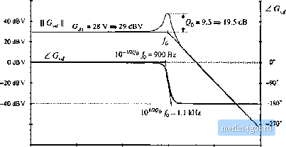
10 Ki 100 Hi IkUz

Fig. 9.24 Converter small-signal comrol-to-output transfer function (7, (jesign exannple,

10 kHz lOOkHz

C.,(s) = G, --l +

By equating like coefficients in Eqs. (9.47) antl (9.48), one finds that the dc gain, corner frequency, and Q-factor are given by

t;=0 = 28V

e.= R\/Y = 9.5 19.5 dB

(9.49)

In practice, parasitic loss elentents, such as the capacitor equivalent series resistance (esr). would cause a lower Q-factor tt) he observed. Figure 9.24 contains a Bode diagram of G.Js). The open-l(Xip line-to-output transfer function is

(9.50)

This transfer function contains the same poles as in Gs), and can be written in the normalized form

(9.S1)

with G o = D. The open-loop output impedance of the buck converter is

l+s+.iLC

(9.52)


Load current variation

ac line varialion


vanalion


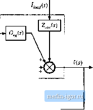
Convener power stage

fig. 9.2s System bioclc diagram, design example.

Use of the.se e(]uatioiis to reptesent the converter in block-diagratri form leads to the complete systetn block diagram of Fig. 9.25. The loop gain of the system is

Substitution ofEq. (9.48) into (9.53) leads to

aSs)H(s) V

(9.53)

(5.54)


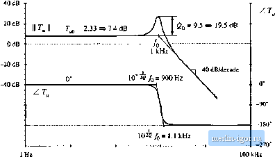
10 Нг

100 Hi

1кНг

10 Ш£

Fig. 9.26 Uncompensated loop gain design exatnple.


1 2 3 4 5 6 7 8 9 10 11 12 13 14 15 16 17 18 19 20 21 22 23 24 25 26 27 28 29 30 31 32 33 34 35 36 37 38 39 40 41 42 43 44 45 46 47 48 49 50 51 52 53 54 55 56 57 58 59 60 61 62 63 64 65 66 67 68 69 70 71 72 73 74 75 76 77 78 79 80 81 82 83 84 85 86 87 88 89 90 91 92 93 94 95 96 97 98 99 100 101 102 103 104 105 106 107 108 109 110 111 112 113 114 115 116 117 118 [ 119 ] 120 121 122 123 124 125 126 127 128 129 130 131 132 133 134 135 136 137 138 139 140 141 142 143 144 145 146 147 148 149 150 151 152 153 154 155 156 157 158 159 160 161 162 163 164 165 166 167 168 169 170 171 172 173 174 175 176 177 178 179 180 181 182 183 184 185 186 187 188 189 190 191 192 193 194 195 196 197 198 199 200 201 202 203 204 205 206 207 208 209 210 211 212 213 214 215 216 217 218 219 220 221 222 223 224 225 226 227 228 229 230 231 232 233 234 235 236 237 238 239 240 241 242 243 244 245 246 247 248 249 250 251 252 253 254 255 256 257 258 259 260 261 262 263 264 265 266 267 268 269 270 271 272 273 274 275 276 277 278 279 280 281 282 283 284 285 286 287 288 289 290 291 292 293 294 295 296 297 298 299 300