
|
| |
|
Строительный блокнот Introduction to electronics 40 dB 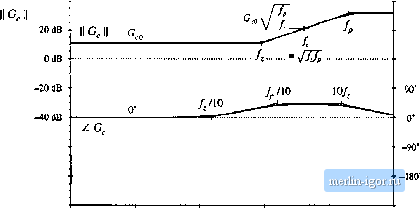 I Hz 10 Нг. ] kHz to kHz 100 Шг Fig. 9.27 ID compeiiNutor triinsfer function G, design extinipiL;, The closed-loop disturbance-to-output transfer functions are given by Eqs. (9.5) and (9.6). The uncompensated loop gain 7jj(.v), with unity compensator gain, is sketched in Fig. 9.26. With GJi) = i, Eq. (9.54) can be written T (.0 = 7;- where the dc gain is (9.55) (9,56) The uncompensated loop gain has a crosstwer frequency of approximately I.S kHz, with a phase margin of less than five degrees. Let us design a compensator, to attain a crossover frequency of/ = 5 kHz, or one twentieth of the switching frequency. From Fig. 9.26, the uncompensated loop gain has a magnitude at 5 kHz of approximately T (/ (4) = 0.093 -20.6 dU. So to obtain unity loop gain at 5 kHz, our compensator should have a 5 kHz gain of+20.6 dB. In addition, the ct)mpensator should improve the phase margin, since the phase t)f the uncompensated loop gain is nearly -180° at 5 kHz. So a lead (PD) compensator is needed. Let us (sotnewhat arbitrarily) choose to design for a phase margin of 52°. According to Fig. 9.13, this choice leads to closeddoop poles having a g-factor of 1. The unit step response, Fig. 9.14, then exhibits a peak overshot)t of 16%. Evaluation of Eq. (9.36), with/ = 5 kllz and 0 = .52°, leads to the following compensator pole and zero frequencies: (9,57) To obtain a ctimpensator gain of 20,6 dB 10.7 at 5 kHz, the low-frequency compensator gain must be 40 dB 20 dB OdB -20 dB 0 dB SA l9JdB J\jQ = - 19.5 ................................................................. 1 кНг Л -. 1.7 kHz 5 kHz 900 Hz 170 Hz  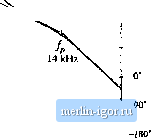 1,4kHzi[7 kHz uSiz-......Y... :- -270* 1 Hz 10 Hz 100 Hz I kHz Fig. 9.28 The compeiLsuted luop gain of Eq, (9.59), 10 kHz 100 kHz V Л (9,58) A Bode diagram of the PD cotnpeiisatcjr magnittide and phase is sketched in Fig. 9.27. With this PD controller, the loop gain becomes 7-(.v)=7-,G 1 +7: (9.59) The compensated loop gain is sketched in Fig. 9.28. It can be seen that the phase of T{.;) is approximately eqnal to 52° over the frequency range of 1.4 kHz to 17 kHz, Hence variations in component values, which canse the crossover frequency to deviate somewhat from 5 kHz, should have litde impact on the phase margin. In addition, it can be seen from Fig. 9.28 that the loop gain has a dc magnitude of ТдО.у I .7 dB. Asymptotes of the quantity 1/(1 +Г) are constructed in Fig. 9.29. This quantity has a dc asymptote of-18.7 dB. Therefore, at frcqticticics less than 1 kHz, the feedback loop attenuates output voltage disturhances by 18.7 dB. Forexample, suppose that the input voltage .(f) contains a 1(X) Hz variation of amplitude 1 V. With no feedback loop, this disturbance would propagate to the output according to the open-lt)op transfer function Gy(i), given in Eq. (9.51). At 1Ш Hz, this transfer function has a gain essentially equal to the dc asymptote D = 0.536. Therefore, with no feedback кюр, a КЮ Hz variation of amplitude 0.536 V would be ohsetved at the output. In the presence of feedback, the clo.sed-loop line-to-output transfer function ofEq. (9.5) is obtained; for our example, this attenuates the 1Ш Hz variation by an additit)nal factor of 18.7 dB = B.6. The 1Ш Hz output voltage variation now has magnitude 0.536/8.6 = ().()62V. The low-frequency regulation can be further improved by addition t)f an inverted zero, as discussed in Section 9,5.2. A PID controller, as in Section 9.5,3, is then obtained. The compensator transfer 2g = 9.S=J 19.5 dB 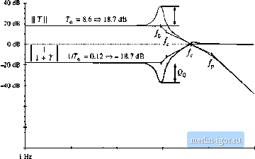 10 Hz IWHz lk№ Fig. 9.29 Con.flructioii o( l/[ I + 7) lor tlie №-e()npen. ted design exiimpEo of Fig. 9,2S. function becomes too kHz (9.Й0) The Bode diagram of this compensator gain is illustrated in Fig. 9.30. The pole and zero frequencies /, and are unchanged, and are given by Eq. (9.57). The raidbandgain is chosen to he the same as the previous Gjfl, Eq. (9.58). Hence, for frequencies greater than Jj, the magnitude of the loop gain is 40 dB 20 dB OdB f -MdB dB 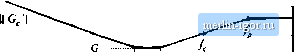 457decade Jl-j,4S7deC 4/10 -180 1 Hi 10 Hi 100 Hi I к Hi tig, 9.30 HD compensator tiantter futvction. Eq. (9.60). 10 kill too kHz |