
|
| |
|
Строительный блокнот Introduction to electronics where G = 0,05, and J\ = C(J/2m = 400 Hz. What is lhe steady-state value of the error voltage ()? Hxplain your reasoning, (b) Determine the steady-state valtie of the main output voltage V. (c) Esiimale the sleady-state value of the auxiliary output voltage Vj, 64:3 J L = 600pH* Fig, 9.41 Flyback cnnverter system of Problem 9.2. © hoiaied transistor gate driver 220 pF -f- J- 100 iF* /, = 200 kHz ms) Ш OJ. Pulse-widllt modulator G,(s) V = 4V Compensator Reference input 93 In the b sl convener system t>f Fig. 9.42, all elements are ideal. The compensator has gain Boost converter 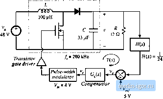 Fig. 9.42 Boost converter system of Prublenn 9.3. Reference input (a) ConstriiCt the Bode plot of the loop gain T(s) magnitude and phase. Label values of all corner frequencies and Q-factors, as appropriate. (b) Determine the crossover frequency and phase margin. Problems (c) Conslrutl the Bode dingrum of (he magnLliide of 1/(1 + 7, using the algebrn-on-the-graph method. Label values uf all corner frequencies and g-factors, as appropriate. (d) Conslrucl Ihe Bode diagj-am of the magnilude of Ihe ciosed-liwp line-Ui-oiitpiit Irnnsler function. Label values of all corner frequencies and -factors, as appropriate. A certain inverter system has Ihe following loop gain and Ihe following open-loop line-lo-oulput transfer func tion 0,/.0 = C,o where j = tOOO rad/sec = 4000 rad/rec COi = 500 rad/scc СЙ, = 24000 rtvd/sec The gain ofthe feedback connection is H{s) = 0.1 <a) Sketch the magni lade and phase asymptotes ofthe loop gain T(.rt. Determine numerical values ofthe cmssover freqtiency in Hz and phase margin in degrees. (b) Ctmstruct the magnitude asymptotes of the closed-loop line-to-(>utpLLt Iransfer function. Label imporiant features. (c) Construct the magnitude asymptotes ofthe closed-loop transfer function from the reference voltage to the outpul voltage. Label important features. The forward converter system of Fig. 9.43(a) is constructed with the element viiiues shtjwn. The quiescent value of the input voltage is V - 380 V.The transformer has turns raliii h/Hj = 4.5, The duty cycle produced by the pulse-widlh modulator is restricted lo the range 0 5 d(,t) £ 0.5. Within this range, (/(f) follows die control voltage v.(i) according to withV =3V. (a) Delermine the quiescent values of: the duly Cycle D, the oulpul voltage V, and the control voltage (h) The op-amp circuit and feedback connection can he modeled using Ihe Ькюк diagram illustrated in Fig. 9.43(b), wilh H(.v) = R/{R + fi). Dctcmimc the transfer functions G(s) and Gs). (c) Sketch a block diagram which models the small-signal ac variations ofthe complete system, and determine the Iransfer function of each block. HiiiK the transformer raagnetiiing inductance has negligible influence on the converter dynamics, and can be ignored. The small-signal models of the forward and buck ctmverters are similar. (d) Construct a Bode plot of the loop gain magnitude and phase. What is the crossover frequency? What is die phase margin? (e) Conslrucl the Bode plot ofthe closed-loop line-to-output iransfer function magnitude Isolated transistor gate driver istorf \ = iiO kHz IJnF Puhe-mdik modulator 5.6 Ш V4- S 8k8kQ > 182 кП 5.1V ОДл)
G,0) Hg. 9A3 Foi-ward converter system of Problem 9.5: (a) system Jiagram. (b) modeling tlie op amp circuit using a block diagram. Label important features, What is the gain at Ш Hz. At what frequency do disturbances in have the greatest Influence on die output vohage 9.6 In the voltage regulator system of Fig. 9.43, described in Problem 9.5, the input voltage v(/) contains a 120 Hz variat:ion of peak amplitude 10 V. (a) What is tlie amplitnde of tlie resulting 120 Hz variation in v(/)? (b) Modify tlie compensator network such that the 120 Hz output voltage variadon has peak amplitude less than 25 mV. Your moditlcarion should leave the dc out:put voltage unchanged, and should result in a crossover frequency no greater than 10 kHz. 9.7 Design of a boost converter with current feedback and a PI compensator. In some applications, it is desired to control the converter input: terminal current waveform. The boost converter system of Fig. 9.44 contains a feedback loop which causes the converter input current ij,()to be proportional lo a reference voltage Iff/O. The feedback conuection is a curreni sense circuit having gain H(s) = 0.2 volts per ampere. A conventional ptilse width modtilator circtiit (Fig. 7.63) is employed, having a sawtooth wave- 500 fiH |
|||||||||