
|
| |
|
Строительный блокнот Introduction to electronics Pmhiems 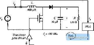
Compensator Reference input His) iis) Fig, 9.44 Boost converter system with cnn-ent ledback, Problem 9,7. form with peak-peak amplitude of = 3 V. The quiescent viiliies of [he inputs are: = 120 V, 2 V, All elements are iJeal, (a) (bJ Determine the quiescent values D. V, and f,. Delermine the small-signal transfer function d(s} (c) Sketch the magnitude and phase asymptotes of the uncompensated (C/v) = 1) bop gain. (d) It is desired to obtain a loop gain magnitude of at least 35 dB at 130 Vh, while maintaining a phase margin of at least 72°. The crossoverfrequency should be no greater than 10= 10 kHz, Design a PI compensator lhat accomphshes this. Sketch the magnilude and phase asymptotes ot the resulting loop gain, and label important features. (e) For your design of part (d), sketch the magnitude of the closed-loop transfer function Label important features. 9Ji Design of a buck regulator tt> meet ckTsed-kx>p output impedance specifications. The buck converter with contrtd system illustrated inFig. 9.45 is to be designed to meet the following specifications. The closed-loop output impedance should be less than 0.2 over the entire frequency range 0 to 20 kHz. To ensure that the transient response is well-behaved, the poles ofthe closed-loop transfer functions, in the vicinity of the crossover frequency, should have -factors no greater than unity. The quiescent load current fjjjj, can vary from 5 A to 50 A, and the above specifications must be met for every value of/[дд in this range. For simplicity, you may assume that the input voltage vg does not vary. The loop gain criissover frequency may be chosen to be no greater than 10, or 10 kHz. You may also assume that all elements are ideal. The pulse-widlh modulator circuit obeys Eq, (7.173). (a) What is the intended dc outpul voltage Vl Over what range does the effective load resistance , vary? 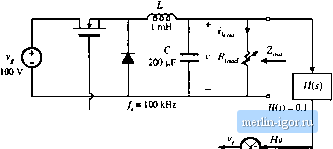 Transistor A gate driver i\
l/ = 4 V Compensator Fig. 9.45 Buck regulator system. Problem y.S (b) Conii[ruL4 lhe magniiiiJe asymptotes оГ the open-loop output impedaDCe Z j(j), Over what range ortreqtienties is the otilput irapeilance speL-ifitaliiin nol mel? Hence, deduce htiw large the minimum loop gain must be in magnitude, such that lhe closed-loop output impedance meets lhe specification. Choose a suitable crossover frequency f;,. (c) Design a compensator network ti,f.v> such that all specifications aie met. Additionally, the dc loop gain 71i) should be at least 20 dB, Specify the following: (i) Yourchoice for the transfer function GJs) (ii) The worsl-case closed-loop Q (iii) Bode plots of the loop gain T{s\ and lhe closed-loop output impedance, for load currents of 5 A and 50 A. What effect does variation of have on the closed-loop behavior of your design? (d) Design a circuit using resistors, capacitors, and an op amp to realize ytjur compensator transfer function CJs). 9S Design of a buck-boost voltage regulator. The buck-boost converter of Fig. 9.46 operates in the conlinu- atis conduction mode, vfith the element values shown. The nominal input voltage is - 48 V, and it is desired to regulate the output voltage at -15 V. Design the best compensaior tliat you can, which has high cnjssover frequency (btil no greater than lOSc ()f the swilching frequency), large loop gain over the bandwidth of the feedback loop, and phase margin of at least 52°. fig. 9.46 Ruck-boost voltage regulator system. Problem y.9.  Transislo gate dri
V =2\ Compensator (a) Specify [he required value of H. Sketch Bode plots ofthe uncorapeiisated loop gain magnitude and phase, as well as [he magnilude and phase of your proposed compensator transfer function GJis). Label the important features of your plots. (b) Construct Bode diagrams t)f the magnitude and phase of your compensated loop gain T(s), and also of the magnitude i)f the quantities J /(l + J) and 1/(1 + T). (c) Discuss your design. What prevents you fmm further increasing the cro.ssover frequency? How large is the loop gain al Ш Hz? Can you obtain more loop gain al 120 Hz? 9.10 The loop gain of a certain feedback system is measured, using voltage injection at a poin[ in the forward path of the loop as illustrated in Fig. 9.47(a). The data in Fig. 9.47(b) is obtained. What is 7i(i) ? Specify TXs) in factored pole-zero form, and give numerical values lor all important features. Over what range of frequencies does the measurement give valid resuhs. (J!)p,(S)pj  60 dB 40 dB 10 dB -20 dB -ISO-
100 Hi lolthi 1 MHz Fig, 9.47 Experimental measurement of loop gain, Problem 9.10; (a) measurement via voltage injection, (b) measured data. |