
|
| |
|
Строительный блокнот Introduction to electronics Convener model © © 1 :D Converter model  ТЛЛГ Fig, 10.3 Siimll-signal eqiiiviilent ilmM iTiodel.s of tlie bgtk tunverter: (ii) bask toiiverier model, (Ъ) with adOilioti iif input filter. 10.1.2 The Input Filter Design Problem The situation faced by the design engineer is, typically as follows. A switching regulator has been designed, which meets performance specifications. The regulator was properly designed as discussed in Chapter 9, using a small-signal model of the converter power stage such as the equivalent circuit of Fig. 10.3(a). In consequence, the transient response is well damped and sufficiently fast, with adequate phase margin at all expected operating points. The output impedance is sufficiently small over a wide frequency range. The line-to-output transfer function G(s), or aiid!osu.4ceplibility, is sufficiently small, so that the output voltage remains regulated in spite of variations in f(t). Having developed a good design that meets the above goals regarding dynamic response, the problem of conducted EMI is then addressed. A low-pass filter having attenuation sufficient to meet conducted EMI specifications is constructed and added to the converter input. A new problem then arises: the input filter changes the dynamics of the converter. The transient respt)nse is mtxiified, and the control system may even become unstable. The output impedance may become large over some frequency range, possibly exhibiting resonances. The audiosusceptibility may be degraded. The problem is that the input filter affects the dynamics ofthe converter, often in a manner that degrades regulator performance. For example, when a single-sectitm L-C input filter is added to a buck converter as in Fig. 10.2(a), the small-signal equivalent circuit model is modified as shown in Fig. 10.3(b). The input filter elements affect all transfer functitms of the converter, including the control-to- 40 dB Fig. 10,4 Coiim>l-lu-oot-put transfer functions predicted by the equivalent circLiii models of Fig. 10.3. Dashed iitws: withuut input filter [Fig, Ю.ЗСа)]. Solid lines: with input tiiter [Fig. 10,3(b). 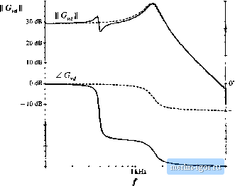 100 Hz -540- tOlcHz output transfer fimctioti GJ.s), the line-to-output tran.sfer function (*). and the converter output impedance Zf,s). Moreover, the influence of the input filter on these transfer functions can be quite As an illustration, lets examine how the control-to-output transfer function Gj((s) of the buck cotiverter of Fig. 10.1 is altered when a simple L-Cinput filter is added as in Fig. 10.2. For this exatnple, the elemetit values are chosen U> be: D = 0.5, L = 100 дН, С = 100 f(F, = 3 i2, L,.= 330 дН, Cy= 470 pP. Figure 10.4 contaitis the Btnie plot of the magnitude and phase of the control-to-output transfer function G(s). The dashed lines are the magnitude and phase before the input filter was added, generated by solution of the model of Fig. 10.3(a). The complex poles of the conveiter output filter cause the phase to approach - 180 at high frequency. Usually, this is the model used to design the regulator feedabck loop and to evaluate the phase margin [see Chapter 9). The solid lines of Fig. 10.4 show the magnitude and phase after addition of the input filter, generated by solution of the model of Fig. 10.3(b). The magnitude exhibits a glitch at the resonant frequency of the input filter, and an additional - ЗйО of phase shift is introduced into the phase. It can be shown that G.Js) now contains an additional complex pole pair and a complex right half-plane zero pair, associated with the input filter dynamics. If the crossover frequency of the regulator feedback loop is near to or greater than the resonant frequency of the input filter, then the loop phase tnargin will become negative and instability will result. Such behavior is typical; consequently, input filters are notorious for destabilizing switching regulator systems. This chapter shows how to mitigate the stability problem, by introducing damping into the inpul filter and by designing the input filter such that its output impedance is sufficiently small [9-21]. The result of these measures is that the effect of the input filter on the control-to-output transfer function becomes negligible, and hence the converter dynatnics are much better behaved. Although analysis of the fourth-order system of Fig. l().3(b) is potentially [jiiite complex, the approach used here simplifies the problem through use of impedance inequalities involving the converter input impedance and the filter output impedance [9,10]. These inequalities are based on Middlebrooks extra element theorem of Appendix C. This approach allows the engineer to gain the insight needed to effectively design the input filter. Optimization of the damping networks of input filters, and design of niuitiple-section filters, is also discussed. 10.2 Effect of an Input Filler on Converter Transfer Function. © Input filter Converter Controller Fig. m.S Addition of an input filter to a switcliing voltage regulator system. 10.2 EFFECT OF AN INPUT FILTER ON CONVERTER TRANSFER FUNCTIONS Tiie tontrol-to-output transfer function G C ) is defined as follows: PCs) (10.3) Tlie eontrol-to-output transfer functions of basic CCM converters with no input filters are listed in Section S.2.2. Addition of an input filter to a switching regulator lead.s to the sy.stem illustrated in Fig. 10.5. To determine the control-to-output transfer function in the presence of the input filter, we set v(s) to zero and solve for v(s)/d(s) according to Eq. (10.3). The input filter can then be represented simply by its output impedance ZJs) as illustrated in Fig. 10.6. Thus, the input filter cim be treated as an extra element having impedance Z (s). In Appendix C, Section C.4.3, Middlebrooks extra element theorem is employed to determine how addition of the input filter modifies the control-to-output Uansfer function. It is found that the modified control-to-output transfer function can be expressed as follows [9]: (Ш.4) Fig, 10,6 Detefrtlinarion of the contfol-to-output transfer Zi) function C ,(.i) for the system of Fig. 10.5, 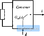 |