
|
| |
|
Строительный блокнот Introduction to electronics 30 dBIJ lOdBfl OdBQ -10 dBQ -20 dBQ 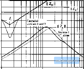 I Шг ШкНг 100 кШ Fig. 10.27 Comparison of the impedance design criteria Zfjts-)) \\ and i:,jO №) II, Eq, (10,13), with the filter output impedance jj ZJJtii) \\. Solid line: j Z(/u)) (j of cascaded design. Dashed line: \\Zfja) ( of section 1 aloiie, raateiy 1С) dBil, or roughly 3 Q. The impedance design criteria (10.13) are also shown, and it can be seen that the filter meets these design criteria. Note the absence of resonances in i Z (j(jJ) . The effect of stage 2 on ZVi) \\ is very small above 40 kHz [where inequalities (10.45) ate very well satisfied], and has moderate-to-smail effect at lower frequencies. It is interesting that, above approximately 12 kHz, the addition of stage 2 actually decreases \\ Zfjia) , The reason for this can be seen from Fig. C.8 of Appendix C: when the phase difference between Z-ZJjbi) and ZiZfJui) is not too large (< 90°), then the 1/(1 + ZJZ term decreases the magnittide of therestilting Zfj(u) \\. As can be seen from the phase plot of Fig. 10.26, this is indeed what happens. So allowing II Zfj<£>) to be simiiar in magnitude to Zijfii) \\ above 12 kHz was an acceptable design choice. The resulting fiiter transfer function is illustrated in Fig, 10,28. It can be seen that it does indeed attain the goal of SO dB attenuation at 250 kHz. Figure 10.29 compares the single stage design of Section 10.4.1 to the two-stage design of this section. Both designs attain 80 dB attenuation at 250 kHz, and both designs meet the impedance design criteria of Eq. (10.13). However, the single-stage approach requires much larger filter elements. 10 J SUMMARY OF KEY POINTS SvvLl-ching converters usually recjuire inpul fillers, lo reduce conducted eleciromagnelic inlerference and possibly also to meet Tequtieinenis ctrnterning condutled suscepitbtltty. AJdilion of an inpul filLer lo a -converler aUeis ihe -conlrol-UJ-oulpul and other Iransfer runL4ions of ihe converter. Design of the Lunverter control syslern must a-ccoLinL for ihe effecls t)f ihe inpul filter. If ihe inpLil filter is noi dampeJ, ihen il lypically iniroduces Lomplex poles anJ RHP zeroes into the converter conlrol-to-outpul Iransfer funclitm al ihe resontinl frequencies tjflhe input Tiher If ihese resonanl frequenLies шге lower than ihe LTOssover frequency of ihe controller loop gain, ihen the phuse margin will become negative und the reguklor w [11 be unslable 20 dB OdB -20 dB 0 dB dB -SOdB -100 dB 120 dB -at 250 kHz IkHz 10 kHz iOOkHz Fig. 10.2Я Input Ttker ttansfer function, cascaded two-section design. , MHz 330 ЦН 470 hF 0.fi7 ns 1200 цР 2 Л 0.65 n 2,9 цН 1 5.8 ixH 11.7mf 1.9 Й -ЛЛг- nL 15.6 цН -гвтпр!- £-1 31.2 цН 6.9 mF FIfi. in.29 Compaiiion of singlo-scction (a) and two section (b) inpul ftlterdeMgiis. Both designs meet the design criteria (10,13), and both enhibil SO dIt of attenuation at 250 kHz. 4. The input fiher tan be designed so that it does not significantly change the converter t;ontrol-to-output and other transfer functions. Impedance inequalities (10. li) give simple design criteria that guarantee this. To meet these design criteria, the resonances of the input filter must be sufficiently damped. 5. Optimization of the damping networks of single-set;tion filters can yield signifit;ant savings in filter element size. Equations for optimizing three different filter sections are listed, 6. Substantial savings m fdter element size can be realized via t;ascading fdter sections. The design of nonin-terat;ting cascaded filter sections can be achieved by an approach similar to the original input filter design method. Impedance inequalhies (10.45) give design criteria that guarantee that interactions are not substantial. References [Ij M. Nave, Ftmer Line Filler Design fur Switched Mode Rower Supplies, New York: Van Nostrand Rein- hold. I??l. [2] De,4ign Guide for Electromagnetic Interference (EMI) Reduction in Power Supplies, MlL-HDBK-24] B, U.S. Department of Defense, April 1 1981. [3] C. Мли511л\г The Gtiide to the EMC Directive S9/S36/EEC, New York: IEEE Press, 1992. [41 P. Deoalue and J. Hamelin, Electromagnetic Compatibility, Oxford: Oxford University Press, 1993. [5] R. Redl, Tower Electronics and Electromagnetic Compatibility, IEEE Power Electronics .Specialists Conference, 1996 Record, pp. 15-21. [6] P. R. WiLLTOL-k. J. A. Fereeiea. j. D. VakWyk. An Experimental Approach to Investigate the Generation and Propagation of Conducted EMI in Conveners, IEEE Power Electronics Specicili.its Conference. I99S Record, pp. 1140-1146. [7] L. Ro.ssETTO, S. Buso and G. Spiazzi. Conducted EMI Issues in a 600W Single-Phase Boost PFC Design, IEEE Tran.sactions on Industry Applications, Vol. 36, No. 2, pp. 378-585, March/April 2(ХЮ. [й] F, Dtts Rei.s, j, Seeastia!4 and J. Uleda, Determination of EMI Emissions in Power Factor Preregula-tors by Design, IEEE Power Electronics S!?eciaU.sts Conference. 1994 Recoid, pp. 1117-1126. [9] R. D. Middlebrook, Input Filter Considerations in Design and Application of Switching Regulators, IEEE Ituhi.itiy Applications Society Annual Meeting. 1976 Record, pp. 366-3S2. [10] R. D. MtDDLEBROUK, Design Techniques for Preventing Input Fdter Oscillations in Switched-Mode Regulators, Proceedings of Powercon 5, pp. A3.1 - A3.16, May 1978. (11) T. Pheus and W. Тлте, Optimizing Passive Input Filter Design, Proceedings of Powercon 6, pp. G 1.1-G 1.10, May 1979. [12] Y. jAit] and R. Erickson, Physical Origins of Input Filter Oscilladons in Current Programmed Converters, IEEE Triin.mclions on Pttwer Electronics. Vol 7, No. 4, pp. 725-733. October 1992. [13] S. Erich and W. Polivka, Input Filter Design for Current-Programmed Regulators, IEEE Applied Power Electronics Conference, 1990 Proceedings, pp. 781-791, March 1990. |