
|
| |
|
Строительный блокнот Introduction to electronics [\4\ N. SoKAL. System Oscillatioits Ciiiscd by Ncganvc Input Rcsistaucc at ttic Power Input Pon of a Switching Mode Regulator, Amplifier, Dc/Dc Ccmvcrtct, or Dc/Лс Inverter, IEEE Power Elearonics Specialisis Conference, 1973 Record, pp. 138-140. (15] A. K.1sl0vski, R. Redl, and N. Sokal, Dyncimic Analysis of Switching-Mode Dc/Dc Converlers, New York: Van Nostrand Rcinhold, Chapter И), 1991. [16] S. Kelk,\e and F. Lei:, A Novel Input Filter Compensation Scheme for Switching Regulators, IEEE Pnwer Electronics Specialists Conference, 19S2 Record, pp. 260-271. [17 R. Ericksok, Optimal Single-Resistor Damping of Input Filters, IEEE Applied Power Electronics Conference. 1999 Proceedings, pp. 1073-1097, .March 1999. [18] M. Flokez-Lizarraga and A. F. Witulski, Input Filter Design for Multiple-Module DC Power Systems, IEEE Transactions on Pcnver Electronics, Vol 11, No. 3, pp. 472479, May 1996. I19j V. VLATKOVlt, D. BOROJEVl*; and F. Lee, Input Filter Design for Power Factor Conrcetion Circuits, IEEE Transactions on Power Electronics. \ol 11, .\o.l,pp. W9-205, January 1Ш. [20] F. Yuan, D, Y, Chen, Y. Wu and Y, Chen, A Procedure for Designing EMI Filters for Ac LincApplica-doiis, IEEE Transactions on Power Electronics. Vol 11, No. 1, pp. 170-181, January 1996. [21] G. Spiazzi and j, Pomilih, Interaction Between EMI Filter and Power Factor Prcrcgulators with Average Current Control: Analysis and Design Considerations, IEEE Tran.ioctions on InJuslriol Electronics, Vol. 46, No. 3, pp. 577-5M,Jtiite 1999. Problems It is requited to design an input filter for the ПуЬаск converter of Fig. 10.30. The maximum allowed ainplitudc of switching harmonics of t;,(f) is 10 )iA rms. Calculate the required attenuation of tlic filter at die switching frequency. 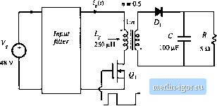 й = 0.3 I = 200 Шг Kig, 10,30 Flyhack converter, Problems 10.1, 10.4, 10.6, 10.8, and 10.10. 10.2 In the boost convener of Fig. 10.31, the input filter is designed so that the maximum amplitude of switching harmonies of i ,(0 is not greatcrthan 10 цА rms. Find the required attenuation of the filter at the switching frequency. 10.3 Derive the expressions forZ and in Table 10.1. 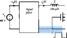
Д = 0,6 - 200 kHi Fig. m.3i Boost converter, Pioblems 10.5, 10.7, and 10,9. 104 The input Iilter for the flyback converler of Fig. 10.30 к designed using a single iy-Cy section. The filter is damped using a resistor Rf\n series wilh a very large blocking capacitor Q, (a) Sketch a small-signal moJel of the flyback converter. Derive expressions for ?.(s] and Z.J,s) using your model. Sketch the magnitude Bode plots of iy and Zj, and label till salient features. (I)) Design the inpul fiber, i.e., select the values uf ly> Cp and Pf, so thai; (0 the filler allenualion al the switching frequency is yl least 100 dB, and (i/J the mtignitude of the tiller output impedance Z (j) sadsfies the conditions IJjdi] \\ < 0.31 ZC/tu) , Ц г Ош) < 0.3 Ц lijijvi) j], for all frt;-ijuencies. (c) Use Spice simulations to verify thai the filler designed in pari (h) meets the specifications. (d) Using Spice simuliilions. plot the converter control-to-oulput magniluJe and phase responses without the inpul fiber, iind with the filler designed in part (bJ. Comment on the changes iniru-ducedby the filter. lO.S II is required to Jesign the input filler for the boo.sl converter of Fig, 10,31 tising a single LpC section. The filter is damped using a resistor in series wilh a very large blocking capacitor C,. (a) Sketch the magnitude Bode plots of 7fji,s) and Zfj) for the boost converter, and label all salient features. (b) Design the input filter, i.e.. Select the values of Lp Cp and Rp so ihiil: (i) the filler allenualion al the switching frequency is at least SO dB, and {ii) the magnitude of the filter оифш impedance Zp) sLitisfies the conditions Zjjin) \\ < 0.2 2,/0)) , Zjjia) \\ < 0.2 ZOa ) ll> for all frequencies. (c) Use Spice simulations lo verify thai the filter designed in part ib) meets the specifications, (d) Using Spice simulations, plot the converter ctmtrt)l-ti>-OLLtput magniluJe and phase responses without the inpul filter, and wilh the filler designed in part (b). Comment on the changes in die conirol-lo-oulpul responses introduceJ by ihe filler. VOA Repeat the filter design of Problem 10.4 using the optimum filter damping approach described in Section 10.4.1. Find the values of fy, Ci fi, and C,y 10.7 Repeat the filter Jesign of rrtjbiem 10.5 using the tiplLmtim filler damping approach of Section 10.4,1. Find the values of Lp Cp Rp anJ IM Repeat the filter design of Problem 10.4 u.4lng the optimum AyZ., parallel damping approach described in Section 10.4.2, FinJ the values uf Lj, Cp Rp and /.[ 10.9 Repeal the filler design of Problem 10,5 using the optimum RyLf, parallel damping approach described in Section 10,4,2. Find the values of Lp Cp Rp and ij. Ж10 It is required to design the input filter for the llyhiict cotiverter of Fig, 10.30 using two filter sections. Eadi filter secdon is damped using a resistor in series with a blocking capacitor. (a) Design the inpul fdter, i.e., select values of all circuit parameters, so that (i) lhe filter attenuation at the swilching frequency is al least 100 dB, and {ii) the magnitude of the filter (mtput impedance Z (i) satisfies the conditions Z (jCi)) Ц < О.ЗЦ Z (jm] Ц, Ц ZJjm) \\ < 0,3 Ц Z/j(U) 1, for a 11 frequencies. (b) Uie Spice simulations to verify lhat the filter designed in part (a) meets the specificadons. (t) Using Spice simulations, plot the converter control-to-output magnitude and phase responses without the inpul filter, and with the filter designed in part (b). Comment on the changes introduced by the fiher. |