
|
| |
Строительный блокнот Introduction to electronics
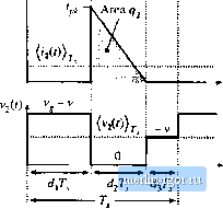 Fig. 11,3 IndQCtor and switch networl; voFtage an(( currenl waveforms, (11.5) The integral is equal to the area under the (((f) wavefonn during the first subinterval. This area is easily evaluated using the triangle area formula: . = *f,(r)rfr4(./,r,)(f j a 1.6) Substitution of Eqs. (11.1) and (11.6) into Eq. (11.5) gives: (11.7) Note that (ii(t))j is not equal to <1<1(0)г,- Since the inductor current ripple is ntit small, it is necessary to sketch the actual input current waveform, including the large switching ripple, and then correctly compute the average as in Eqs. (11.5) to (11.7). The average diode current {ijil)} ks found in a manner similar to that used above for (fj(())j.: (11.Й) The integral s equal to the area under the lj(0 waveform during the second subinterval. This area is evaluated using the triangle area formula: 92 = (11.9) Substitution of Eqs. (11.1) and (11.9) into Eq, (11.8) leads to: {i,it))y-M,(r)) (11,10) Equations (11.3), (11.4), (11.7) and (11.10) constitute the averaged terminal equations of the switch network in the DCM btick-bt)ost converter. In these equations, il remains to express the subinterval length in terms of the switch duty cycle d = d, and the converter averaged waveforms. One approach to finding the subinterval length d is by solving the inductor cuirent waveform. In the buck-boost converter, the diode switches off when the inductor current reaches zero, at the end of the sec- ond subinterval. As aresult, iiO\) = £.(0) = 0, There is no net change in inductor current over one complete switching period, and no net volt-seconds are applied to the inductor over any complete switching period that starts at the time when the transistor is turned on. Therefore, the average inductor voltage computed over this period is zero, Ы>)г, = <{Щ, + = + 0 - 0 (11.1J) even when the converter is not in eqtiilibrium. This eqtiation can be used to find the length of the second subinterval; rf.W=-rf(/)t 0U2} Substitution ofEq. (1 1.12) into Eqs. (11.3), (11.4), (11.7) and (11.10), allows us to obtain simple expressions for the averaged terminal waveforms ofthe switch network in the discontinuous conduction mode: {vi(i)).,=-{v{i)), (11,14) Let us next construct an equivalent circuit corresponding to the averaged switch networlt equations (11.15) and (11.16). The switch network input port is modeled by Eq. (11.15). This equation states that the average inputcurrent {/i(0)j; is proportional to the applied input voltage (v(f)). In other words, the low-frequency components of the switch network input port obey Ohms law: where the effective resistance is RAd,)-jb (11.18) An equivalent circuit is illustrated in Fig. 11.4. During the first subinterval, the slope ofthe inputcurrent waveform is proportional to the input voltage(v,())rj ~ (vj(()y,r, as illustrated in Fig. 11.3. As a result, the peak current i,, the total charge and the average inputcurrent {iyit))f, are also proportional to (V(f))jj,. Of course, there is no physical resistor inside the converter. Indeed, if the converter elements are ideal, then no heat is generated inside the converter. Rather, the power apparently consumed by is transferred to the switch networlt output port. Fig, 11.4 Equivalent circuit that modeis the avea-age waveforms of the switoli input (transistor) port, The switch networlt output (diode) port is modeled by Eq, (11.16), or ШгШгг- (11.19) Note that (vUf-j-Jfi is the average power (/)(()) apparently consumed hy the effective resistor RJdi). Equation (11.19) states that this power flows out of the switch networl; output port. So the switch network consumes no net power-its average input and output powers are equal. Equation (11.19) can also be derived by con.si deration of the inductor stored energy. During die first subinterval, the inductor cunent increases from 0 to In the process, the inductor stores the following energy: (11.20) Here, ijji has been expressed in terras of {v,(f))j. using Eqs. (11.1) and (11.13). This energy is transferred from the source 1 through the switch network input terminals (i.e., through the transistor), to the inductor. During the .second subinterval, the inductor releases all of its stored energy through the switch network output terminals (i.e., through the diode), to the output. The average output power can therefore be expressed as the energy transferred per cycle, divided by the switching period: This power is transferred to the load, and hence
(11.21) (il.22) This result coincides with Eq. (11.19). The average power (p(0) is independent of the load characteristics, and is determined solely hy the effective resistance and the applied switch network input terminal voltage or current. In other words, the switch network output port behaves as a source of power, equal to the power apparently consumed by the effective resistance R. This behavior is represented schematically by the dependent power .source Symbol illustrated in Fig. 11.5. In any lossless two-port network, when the voltage and current at one port are independent of the characteristics of the external network connected to the second port, then the second port must exhibit a dependent power source characteristic [10]. This situation arises in a num- |
||||||||||||||||||||||||||||||||||||||||||||||||||||||||||||||||||||||||||||||