
|
| |
|
Строительный блокнот Introduction to electronics Power input
Control input Fig. 3.1 Switching converter terminal quantities. Power output Power input Power output Fig. 3,2 A swrtdiing convener equivalent ciicuit using dependent soujces, eonesponditig to liqs. (3.3) and (3.4-). These relationships are valid only under equilibrium (dc) conditions: during tran.sients, the net stored energy in the converter inductors and capacitors may change, causing Eqs. (3.1) and (3.2) to be violated. In the previous chapter, we found that we could expres.s the converter output voltage in at] equation of the form V = M(£i)V, (3,3) where M(D) is the equilibrium conversion ratio of the converter. For example, M{D) = D for the buck converter, and M{D) = 1/(1 ~ D) for the boost converter. In general, for ideal PWM converters operating in the continuous conduction mode and containing an equal number of independent inductors and capacitors, it can be shown that the equilibrium conversion ratio M is a function of the duty cycle D and is independent of load. Substitution of Eq. (3.3) into Eq. (3.2) yields (3.4) Hence, the converter terminal current. are related by the same conversion ratio. Equatioi]s (3.3) and (3.4) suggest that the converter could be imxleled using dependent sources, as in Fig. 3.2. An equivalent but more physically meaningful model (Fig. 3.3) can be obtained through the realization that Eqs. (3.1) to (3.4) coincide with the equations of an ideal transformer. In an ideal transformer, the input and output powers are equal, as stated in Eqs. (3.1) and (3.2). Also, the output voltage is equal to the turns ratio times the input voltage. This is consi.steiit with Eq, (3.3f, with the turns ratio taken to be the equilibrium conversion ratio M(D). Finally, the input and output currents should be related by the same turns ratio, as in Eq. (3.4). Thus, we can model the ideal dc-dc converter using the ideal dc transformer model of Fig. 3.3. II The DC Transformer Model 1 : МФ) Fig. 3.3 Ideal dc iransfoiJtier model of a dc-dc convener operating in continuous conduction mode, corresponding to Eqs. (3,1) to (3,4), Fawer \nput ё S Power output Control input This symbol represents the first-order dc properties of any switching dc-dc converter: transformation of dc voltage and current levels, ideally with Ш)% efficiency, controllable by the duty cycle D. The solid horizontal line indicates that the element is ideal and capable of passing dc voltages and currents. It should be noted that, although standard magnetic-core transformers cannot transform dc signals (they saturate when a dc voltage is applied), we are nonetheless free to define the idealized model of Fig. 3.3 for the purpose t)f mt)de]ing dc-dc converters. Indeed, the absence of a physical dc transformer is one of the reasons for building a dc-dc switching converter. So the properties of the dc-dc converter of Fig. 3.1 can be modeled using the equivalent circuit of Fig. 3.3. An advantage of this equivalent circuit is that, for constant duty cycle, it is time invariant: there is no switching or switching ripple to deal with, and only the important dc components of the waveforms are mt)deled. The rules ft)r manipulating and simplifying circuits containing transformers apply equally well to circuits containing dc-dc converters. For example, consider the network of Fig. 3.4(a), in which a resistive load is ctmnected to the converter output, and the power source is modeled by a Thevenin-equiv-alent voltage source Vj and resistance R. The converter is replaced by the dc transformer model in Fig. 3.4(b). The elements Vj and Jf, can now be ptished through the dc transformer as in Fig. 3.4(c); the volt- (a) Л, Fig. 3.4 Example of use of the dc transformer model: (a) original circuit; (b) substitution of switching converter dc transformer model; (c) simplification by referring all elements to secondary side. Switching de-dc converter 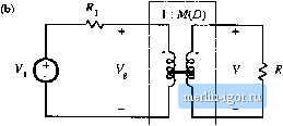 -vv- M(D)V, V <R age source V is multiplied by the conversion ratio Af(D), atid the resistor/f, ismultipliedby M (D). This circuit can now be solved using the voltage divider formula to find the output voltage: (3.5) It should be apparent that the dc traiisforraer/equivalent circuit approach is a powerful tool for understanding networks containing converters. INCLUSION OF INDUCTOR COPPER LOSS ЛЛг The dt transformer model of Fig. 3.3 can be extended, to model other properties t)f the converter. Non-idealities, such as sources of power loss, can be modeled by adding resistors as appropriate. In later chapters, we will see that converter dynamics can be modeled as well, by adding inductors and capacitors to the equivalent circuit. Let us consider the inductor copper loss in a boost converter. Practical inductors exhibit power loss of two types: (i) copper loss, originating in the tesistance of the wire, and (2) core loss, due to hysteresis and eddy current los.ses in the magnetic core. A suitable model that describes the inductor copper loss is given in Fig. 3.5, in which a resistor l is placed in .seties with the inductor. The actual inductor then cnnsists of an ideal inductor, L, in series with the copper loss resistor ff The inductor model of Fig. 3,5 is insetted into the boost converter circuit in Fig. 3.fi. The circuit can now be analyzed in the same manner as used for the ideal lossless converter, using the principles of inductor volt-second balance, capacitor charge balance, and the small-ripple approximation. First, we draw the converter circuits during the two subintetvals, as in Fig. 3.7. ForO < t < DT, the switch is in position 1 and the circuit reduces to Fig. 3.7(a). The inductor voltage Vj(f), across the ideal inductor L, is given by tlg. 3.5 Modeling inductor copper loss via series resistor/f, and the capacitor current tf(t) is ,jO-v--i()?j, (3.6) (3.7) Next, we simplify these equations by assuming that the switching ripples in i{t) and v(t) are small compared to their respective dc components / and V. Hence, /(f) = / and v(f) = V, and Eqs. (3.6) and (3.7) 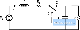 ilB. 3,(i Boost converter circuit, including inductor copper lesistiiitce r,. |
|||||||||||||||