
|
| |
|
Строительный блокнот Introduction to electronics d(t) 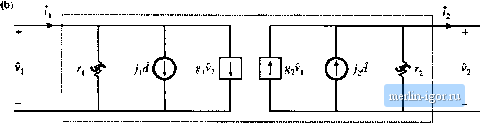 Fig. 11.13 Averaged models of the gsntrul two-switch ntitwork in a tuiSviirtcr operating in DCM: (a) large-signal model, (h) small-signal model, = (U.36> Here, D is the quiescent value of the transistor duty cycle, is the tjiiiescent value of the applied average transistor voltage {v(t))y, etc. The quantities 0), v,(0, etc., are small ac variations about the respective quiescent values, it is de.siied to linearize the average switch network terminal eqnation.s (11.15) and (11.16). Equations (11.15) and (11.16) express the average terminal currents {((r))j, and {(3(/))j, as functions ofthe transistor duty cycle d(t) ~ dit) and the average terminal voltages {v(t)) and (,v.{t))j.. Upon perturbation and linearization of these equations, we will therefore find that /jW and l2(t) are expressed as linear functions ot d(t), vif), and vO)- So the small-signal switch network equations can be written in the following form: t = +Jl?+ilVi 2 = -7 + J2f-t-Sif, (11,37) These equations describe the two-port equivalent circuit of Fig. 11.13(b). The parameters and g. tan be found by Taylor expansion ofEq. (11.15), as de.seribed in Section 7.2.7. The average transistor current (i,(0) ,Eq. (11.15), can be expressed in the following form: (И.ЗЙ) Let us expand this expression in a three-dimensional Tavlor series, about the quiescent operating point n = V, + v.,(r)- v, = V, (lt,39) + higher-order nonlinear terms For simplicity of notation, the angle brackets denoting average values are dropped ш the above equation. The dc terms on both sides ofEq. (1 1.39) must be equal: (11,40) As tisual, we linearize the equation by discarding the higher-order nonlinear terms. The remaining first-order linear ac terms on both sides of Eq. (11.39) are equated: ,(t) = V,{t)-i- + Vj{t)g,i.d(t)j, (11.41) where -df{v V,.Dl V, = V, (11.42) 3f\{v,v D) (11,43) Dli,{i>) d = D KliD) V, ОДДг/) d = 0 (] 1.44) Thus, the small-signal input resistance r, is equal to the effective resistance R, evaluated at the quiescent operating point. This term describes how variatioii.4 in (V(r))j affect (i,(0) , via fi ,(/J). The small-signal parameter is equal to zero, sinee the average transistor current \ii())]-, is independent of the average diode voltage (Vj(f))j,, The small-signal gain describes how duty cycle variations, which affect the value of Rj,(</), lead to variations in {iU))yy In a similar manner, ((f))]-, frotn Eq, (11.16) can be expressed as (11,45) Expansion of the function/jtf . Vj, Ю in a three-dimensional Taylor series about the quiescent operating point leads to f ; V D) + d(i) -i-T- (11.46) + higliei--K3rder nonlinear terms By equating the dc terms on both sides of Eq. (11.46), we obtain The higher-order nonlinear terms are discarded, leaving the following first-order linear ac terms: 7) = fj(f)(-)+fl(05 + ()j2 with Г2 ~~V = 1 = -1- (11.47) (11,4S) (11.49) -dV,- v, = V. (11.50) . 4{v>,v d] SUM) d = D ИЛО)У, <id d = D (11.51) DMRXD) The output resistance describes how variations in(ij(0)r, influence {ij(0)j-j. As illustrated in Fig. 11.14, |