
|
| |
|
Строительный блокнот Introduction to electronics .1С and DC Equivalent Circuit Modeling of tlie Diseonlinuims Conduerion Mode Fig. 11.14 Tlie sinail-Mgnal output resistance Ik determined by the slope of the power source charactcfistio at the quiescent operating point. Load characteristic 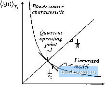 1йЫе 11.2 Small-signal OCM switch inocteJ parameters Switch networlc General two-switch, Fig. 11.7(a) Buck, Rg. 11.16(a) Boost, 2V DR, DR, 2MV, 2 Ш. 2M-1 DMR, DMR, 2V, M-R, M% ----- --i- ---- t Ч n--- (11 \\lD Fig.ll.l6(b) (iW-l)=R, Di M-\)R, M- (M-lfR, D{M-l)R, /j is determined by the slope of the power source characteristic, evaluated at the quiescent operating point. For a linear resistive load, = R. For any type of load, it is true that = MKJiD). The parameters 7; and describe how variations in the duty cycle rf(r) and in the average transistor vt>ltage (l,(f))7 (which influence the average power (/)(/))j.) lead to variations in the average dit>de current (((f)) . Values t>f the small-signal parameters in the DCM switch model of Fig. 11.13(b) are summarized in the top row ofTable 11.2. к small-signal model of the DCM btick-boost converter is obtained by replacing the transistor and ditKle of the converter with the switch mtxlel of Fig. 11.13(b). The result is illustrated in Fig. 11.15. This equivalent circuit can now be solved using conventional linear circuit analysis techniques, to determine the tran.sfer functions and t;ither small-signal quantities of interest. The same small-signal switch model can be employed to inodel other DCM converters, by simply replacing the transistor and diode with ports 1 and 2, respectively, of the two-port model of Fig. 11.13(b). An alternative approach, which yields more convenient results in the analysis of the buck and boost converters, is to define the switch network as illustrated in Figs. 11.16(a) and 11.16(b), re.spectively. These switch networks can also be modeled using the two-port small-signal equivalent circuit of Fig. 11.16(c)l however, new expressions for the parameters f,j, etc., must be derived. Tlie.se expressions are again found by linearizing the equations of the averaged switch network terminal currents. Switch ntwark fmnli-$fgnai or modl Fig. 11.15 Small-signul ac model ofthe DCM buck-boost converter obtained by insertion of the switch network two-port small-slgnul mode] into the original conveiter circuit.
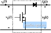 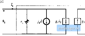 Fig. 11.16 A convenient way to model the switch networks cif DCM buck and boost conveners: (a) defined terminal quantities of ihe DCM buck switch network, (b) defined terminal quantities ofthe boost switch network, (c) two-port small-signal ac model. The model parameters ore given in Table 11.2, Table 11.2 lists the .small-signal parameteis for the buck switch network of Fig. 11.16(a) (middle itjw) and for the boost switch network of Fig. 1 l.lfi(b) (bottom row). Insertion ofthe small-signal two-port model into the DCM buck and boost converters leiids to the equivalent circuits of Fig. 11.17. The small-signal equivalent circuit models of Fig. 11.15 and Fig. 11.17 contain two dynamic elements: capacitor С md inductor L Conti-ol-to-output tr;msfer functions obtainetl by .solving these equivalent circuit models have two poles. It has been shown [2-6] that one ofthe p[)les, due to the capacitor С appeai-s at a l[)w fiequency, while the other pole (and a RHP zero in the са.че of boost and buck- DCM buck switch network imall-sigaal ac nmdel f JdQ ,;,т Tl =. f h h с <v - -оТйг - © DCM boost switch networlt smalt-signal ac model h с R < f Fig, 11Л7 sitieiil-signul ac nitjilds of (a) tfic DCM but:k tortverter, antl (b) the ГХ1!М botist tonvciter, obtnintjd by replacing the switch netwoi-ks defined in Fig. 11.16(a) and (bj with the sniali-signaJ switch model of Fig. 11.16(c), boost converters) tJue to the inductor L, occurs at tnuch higher frequency, close to the converter switching frequency. Therefore, iu practice, the DCM buck, boo.st, and buck-boost converters exhibit essentially single-pole transfer functions, which are negligibly influenced by the inductor dynamics. The small-signal equivalent circuit models have been derived in this section from the large-signal averaged switch network equations (11.15) and (11.16). These equations are based on Eq. (1 1.1 I), which states that the average inductor voltage, and therefore its small-signal ac voltage, is zero. This contradicts predictions of the resulting small-signal models in Figs. 11.15 and 11.17. As a result, we expect that the models derived in this section can be used to predict low-frequency dynamics, while predictions of the high-frequency dynamics due to the inductor L are of questionable validity. Equivalent circuit models that give more accurate predictions of high-frequency dynamics of DCM converters are discussed in Section 11.3. A simple approximate way to determine the low-frequency small-signal transfer functions of the buck, boost, and buck-boost converters is to let the inductance L tend to zero. If i, is shorted in the equivalent circuits ofFigs. 11.15 and 11.17, the model in all three cases reduces to Fig. 11.18. Thiscir- DCM Switch network small-signal лс model с dp R$ Fig. 11.18 l w-frequency ac model obtained by letting Л approach zero, Tlic buck, boost, or buck-boost convert-crs can be motleled, by employing the appropriate piifameters from Table 11.3. |
|||||||||||||||