
|
| |
|
Строительный блокнот Introduction to electronics ЛЛ-!  Fig. Э.10 Circuit whose loop equation is identical tn Eq. 016), obtatned by etiuathig the average inductor voltiige {iJf.) to zero. identical to Eqs. (3.15). 3.3.1 Inductor Voltage Equation W)-0-,-IR.-UV This equation was derived by use of Kirehoffs voltage law to find the indtictor voltage during each sub-interval. The result.s were averaged and set to zero. Equation (3.16) states that the sum of three terms having the dimensions of voltage are equal to (v,), or zero. Hence, Eq. (3.ifl) is of the same form as a loop equation; in particular, it describes the dc components of the voltage.s around a loop containing the inductor, with kwp current equal to the dc inductor current /. So let us construct a circuit containing a k)op with current /, corresponding to Eq. (3.16). The first term in Eq. (3.16) is the dc input vt)ltage V., so we should include a voltage source of value Vas, shown in Fig. 3.10. The second term i.s a voltage drop of value IR;, which is proportional to the current / in the loop. This term corresponds to a resistance ofvalue The third term is a voltage DV, dependent on the converter output voltage. Ft>r now, we can model thi.s term using a dependent voltage source, with polarity chosen to satisfy Eq. (3.16). 3.3.2 Capacitor Current Equation (3.17) This equation was derived using Kirehoffs current law to find the capacitor current during each subinterval. The results were averaged, and the average capacitor current was set to zerti. Equation (3.17) states that the sum of two dc currents are equal to {if), or zero, Hence, Eq. (3.17) is of the same form as a node equation; in particular, it describes the dc components of currents Node Fig. 3,11 Circuit wliose node equation isj identical to Eq. (3,17), obtained by equating the average capacitor current {i.)l< 7ero. = 0 * С :: J J Опшгпсиоп ojEqimakm Circm Model D! V Fig. 3.12 The circuits of Figs. 3.10 and 3.11, til awn together. ЛЛг Fly, ЪЛЪ Equivalenl cin;uit mudelof the boost converter, including a DA dc iransformcr and the inductor wind-(dg resistance R,. flowing into a node connected to the capacitor. The dc capacitor voltage is V. So now let us construct a circuit containing a node connected to the capacitor, as in Fig. 3.11, whose node equation satisfies Eq. (3.17), The second terra in Eq. (3.17) is a current of magnitude V/R, proportional to the dc capacitor voltage V. This term corresponds to a resistor of value R, connected in parallel with the capacittir so that its voltage is Vand hence its current is V/R. The first term is a current Di, dependent on the dc inductor current /. For now, we can model this term tising a dependent current source as shown. The polarity of the source is chosen to satisfy Eq. (3.17). 3 J.3 Complete Circuit Model The next step is to combine the circuits of Figs. 3.10and 3.i i into a single circuit, as in Fig. 3.12. This circuit can be further simplified by recognizing that the dependent voltage and current sources constitute an ideal dc transformer, as discussed in Section 3.1. The DVdependent voltage source depends on V, the voltage actoss the dependent current soiitte. Likewise, the DI dependent ciirrettt .source depends on /, the ctirrent flowing through the dependent voltage source. In each case, the coefficient is D. Hence, the dependent sottrces form a circuit similar to Fig. 3.2; the fact that the voltage source appears on the primary rather than the secondary side is irrelevant, owing to the symmetry of the transformer. They are therefore equivalent to the dc transformer model of Fig. 3.3, with turns ratio liA. Stibstrtution of the ideal dc transformer model for the dependent sources yields the equivalent circuit of Fig. 3.13. The equivalent circuit model can now be manipulated and solved to find the converter voltages and currents. For example, we can eliminate the transformer by referring the voltage source and R resistance to the secondary side. As shown in Fig. 3.14, the voltage source value is divided by the effective turns ratio D, and the resistance R, is divided by the square of the turns mtio, D, This circuit can be solved directly for the output voltage V, using the voltage divider formula: Fig. 3.14 Simplification of tiie et;uiva]eiit cn-cuW of Fig, 3,13, by refeiiing all dements to the .sceottdary side of lite tiansftirmer. 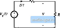 (3.18) This result is identical to Eq. (3.14). The circuit can also be solved dtrectly for the itiductor current /, by referring all elements to the transformer primary side. The result is: (3.19) 3.3.4 Efficiency The equivalettt circuit model also allows us to compute the converter efficiency т. Figure 3.13 predicts that the converter input power is (3.20) The load current is equal to the current in the secondary of the ideal dc transformer, or Dl. Hence, the model predicts that the converter output power is Therefore, the converter efficiency is .!.mJp}l.Lry (3.21} (3.22) Substitutjon of Eq, (3.18) into Eq. (3.22) to eliintnate Vytelds (3.23) This equation is plotted in Fig. 3.15, for several values oi RIR. It can be seen from Eq. (3.23) that, to obtain high efftciency, the inductor winding resistance should be much smaller that DR, the load resistance referred to the primary side of the ideal dc transformer. This is easier to do at low duty cycle, where D is cluse to unity, than at high duty cycle where 1У approaches zero. It can be seen from Fig. |