
|
| |
|
Строительный блокнот Introduction to electronics This page intentionally left blank Inductor Design This chapter treats the design of magnetic elements such as filter inductors, using the method. With this method, the maximum flux density is specified in advance, and the element is designed to attain a given copper loss. The design of a basic filter inductor is discussed in Sections 14.1 and 14.1.5. In the filler induclor application, it is necessary toobtain the required inductance, avoid saturation, and obtain an acceptable low dc winding resistance and copper loss. The geometrical constant is a measure of the effective magnetic size of a core, when dc copper loss and winding resistance are the dominant constraints [1,2]. Design of a filter inductor involves selection of a core having a sufficiently large ftff the application, then computing the required air gap, turns, and wire size. A simple step-by-step filter inductor design procedure is given. Values of for common fertile core shapes are tabulated in Appendix D. Extension of the Amethod to multiple-winding elements is covered in Section 14.3. In applications requiring multiple windings, it is necessary to optimize the wire sizes ofthe windings so that the overall Copper loss is minimized. It is also necessary to write an equatitm that relates the pealt lliix density to the applied waveforms or to the desired winding inductance. Again, a simple step-by-step transformer design approach is given. The goal ofthe K, apprt)ach of this chapter is the design of a magnetic device having a given Cupper loss. Core loss is not specifically addressed in the approach, and is a given fixed value. In the next chapter, the Пих density is treated as a design variable to be optimized. This allows the overall loss (i.e., core loss plus copper loss) to be minimized. 14.1 FILTER INDUCTOR DESIGN CONSTRAINTS A filter induclor employed in aCCIVI biiclt Converter is illustrated in Fig. i4.l(a). In this application, the value of inductance i. is usually chosen such that the inductorcurrent ripple pealtmagnitude A* is a small fraction of the full-load induclor current dc component /, as illustrated in Fig. 14.1(b). As illustrated in Fig. 14.2, an air gap is employed that is sufficiently large to prevent saturation of the core by the peak 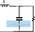 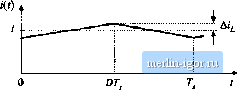 Fig. 14.1 Filter Inductor employed in a CCM buck coEiverter: (a) eifcuit schematic, (b) inductor current waveform. Core reluctance гЖ,
M Air gap reluctance Fig, 14.2 Filter inductor: (a) structure, (b) Enagnotic circuit model, current / + M. Let us consider tlie design of the filter itiductor illustrated in Figs, 14.1 and 14.2. It is assumed that the core and proximity losses are negiigibie, so that the inductor losses are dominated by the Iow-fret]uency copper losses. The inductor can therefore be modeled hy the et[uivitlent circuit of Fig. i4.3, in which R represents the dc resistance of the winding. It is desired to obtain a given inductance L and given winding resistance R. The inductor should not saturate when a given worst-case peak current is applied. Note that specification oiR is equivalent to specification of the copper loss since P =/= R (14.1) The influence of inductor winding resistance on converter efficiency and output voltage is tnotleled in Chapter 3. ЛЛг- Fig, 14.3 Filter inductor equivalent circuit. |
|||||||||||||||||||||||||||