
|
| |
|
Строительный блокнот Introduction to electronics the increased copper ioss and smaiier core size will lead to a higher temperature rise, which may he iinacceptahie. The fill factor also influences the core size. Equation (14.15) reveals how core geometry affects the core capabilities. An inductor capable of meeting increased electrical requirements can be obtained by increasing either the core areaA., or the window area W. Increase of the core area requires additional iron core tnateriai. Increase of the window area implies that additional copper winding tnateriai is einployed. We can trade iron for copper, or vice versa, by changing the core geometry in a way that inaintainsthe of Eq. (14.15). 14,2 A STEP-BY-STEP PROCEDLRE The procedure developed in Section 14.1 is summarized below. This sitnple filter inductor design ргтее-dure should be regarded as a first-pass approach. Numerous issues have been neglected, including detailed insulation requiretnents, cotiductoreddy current losses, tetnperature rise, roundoff of nutnher of turns, etc. The following quantities are specified, using the units noted:
The core ditnensioiis are expressed in cm: Cure cruss-sectional area A (cni) Core window area (cni) Mean length per turn - (m) The use of centitneters rather than ineters requires that appropriate factors he added to the design equations. 1. Determine core size K>-Ul (cm) (W,16) Choose a core which is large enough to satisfy this inequality. Note the values of A . W, and MLT for this core. Theresistivity p of copper wire is 1.724 1(Г* £i-cm at room temperature, and 2.3 10 * fl-cm at 10O=C. 2. Determirte air gap lengtli t = lO (m) (1*17) with Aexpressed in cm. = 4n \0~ H/m. The air gap length is given in meters. The value expressed in Eq. (14.17) is approximate, and neglects fringing flux and other nonidealities. Core manufactureis sell gapped tores. Rather than specifying the air gap length, the equivalent quantity Ак used. Af is equal to the iiiductaiiee, in mH, obtained with a winding of ICXXl turns. When Af is specified, it is the core tnanufacturers responsibility to obtain the cotxect gap length. Equation (14.17) can be tnodified to yield the requited Ay as follows: A=iiHi (jnH/imO turns) (H.I8) where is given in cm, L is given in Henries, imd is given in Tesla. 3. Determine number of turns JdmL. io (14.19) 4. Evaluate wire size A<!i (cm (14.20) Select wire with bare copper area less than or equal to this value. An Atnetican Wire Gauge table is included in Appendix D. As a check, the winding resistance can be computed: 14.3 MULTIPLE-WINDINC, MAGNETICS DESIGN VIA THE METHOD The tnethod can be extended to the са.че of multiple-winding magnetics, such as the transformers and coupled inductors desciibed in Sections 13.5.3 to 13.5.5. The desired turns ratios, as well as the desired winding voltage and curtent waveforms, are specified. In the case of n coupled inductor or flyback transformer, the magnetizing inductance is also specified. It is desired to select a core size, number of turns for eiich winding, and wire sizes. It is also assumed that the tnaximum flux density B, is given. With the K method, a desired copper loss is attained, hi the tnuitiple-winding case, each wind-ing contributes some copper loss, and it is necessary to allocate the available window area among the various windings. In Section 14.3.1 below, it is foutid that total copper loss is minitnized if the window iffea is divided between the windings according to their apparent powers. This result is employed in the following sections, in which anoptitnized method for coupled inductor design is developed. 14.3.1 Window Area Allocation The first issue to settle in design of a multiple-winding tnagnetic device is the allocation of the window area Лу, among the viuious windings. It is desired to design a device having Awindings with turns ratios itf ; П2 i.,; n. These windings must conduct rmscurrents /[, /i 7 tespectively. It should be noted that the windings are effectively in parallel: the winding voltages ate ideally teiated by the turns ratios rms currenl rms current nris current Fig. 14.6 It ia ilesiicd to optimally allocate the window area of и i-wiiiding inagnctic clement to miiiimi/e low-frequency copper losses, with given rms winding currents and tunis ratios. r,(0 VffO (14.12) However, the winding rms currents are determined by the loads, and in general are not related to the timis ratios, The device is represented schematically in Fig. 14,6. The relevant geometrical parameters are summarized in Fig. 14.7(a). It is necessary to allocate a portion of the total window area to each winding, as illnstrated in Fig. 14,7(b). Let O.- be the fraction of the window area allocated towinding /, where 0<C(j< 1 1 + 2+ (14.23) Fig. 14.7 Basic core topokigy, including window area enclosed by core (a). The window is a]l(K;i!ted ti> the various windings lo minimize low-frequency copper lo.ss (b). 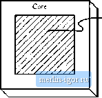 Window area Core mean length per turn [MLT] Wire resistivity p Fill factor A-., Winding 1 altecation Winding 2 allocation etc.  Total window area W. |