
|
| |
Строительный блокнот Introduction to electronics 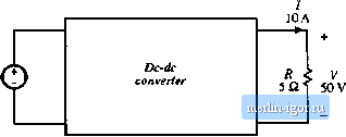 100 V Fig. 1.6 Л simple power processing exsimple: cOnsti uction of a 5Ю W Uc-dc Cunverter, 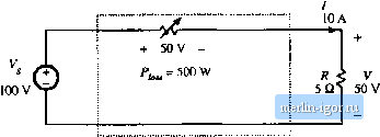 p=1000W 100 V ! + sov Linear amplifier and tiase driver P = 500W 10 A V 50 V /*, =1000W ------------------------ P , = 500W Fig. 1.7 Changing the dc voltage via disslpntivc means: <a) voltage JiviJer, (b) aeries puss rsrgiilator variable resistor, whose value is adjusted such that the required output voltage is obtained. The load current flows through the variable resistor. R)r the specified voltage and current levels, the power P/ dissipated in the variable resistor equals the load power - 500 W. The source V, supplies power = iOOO W. Figure 1.7(b) illustrates a more practical implementation known as the linear series-pass regulator The variable resistor of Fig. 1.7(a) is replaced by a linear-mode power transistor, whose base current is controlled by a feedback system such that the desired output voltage is obtained. The power dissipated by the linear-mode transistor of Fig. l,7(b) is approximately the same as the 5(X)W lost by the variable resistor in Fig. i.7(a). Series-pass linear regulators generally find modern application only at low power levels of a few watts. Figure 1.8 illustrates another approach. A single-pole double-throw (SPDT) switch is connected as shown. The switch output voltage vjt) is equal to the converter input voltage V, when the switch is in position 1, and is equal to zero when the switch is in position 2. The switch position is varied periodically, as illustrated in Fig. 1.9, such that vj,t) is a rectangular waveform having frequencyand period T, = l/f, The duty cycle D is defined as the fraction of time in which the switch occupies position 1. Hence, 0< D< 1. In practice, the SPDT switch is realized using switched-mode seiniconductordevices. J.J Introduclionlo Power Processing 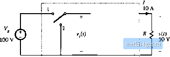 Kig. 1.8 liLstrtiuri (if SPDT switch wliicli chiinge-s the dc compancnt of tile voltage. switch position: ] Kig. I.S Swiieh output vol [age waveform v[l).  which are controlled such that the SFDT switching function is attained. The switch changes the dc component of the voltage. Recall from Fourier analysis that the dc contponent of a periodic waveform is equal to its average value. Hence, the dc component of is vJt)dt = DV, (1.3) Thus, the switch changes the dc voltage, by a factor eqital to the ditty cycle D. To convert the input voltage V, = 100 V into the desired output voltage of V= 50 V, a duty cycle of Z) = 0.5 is required. Again, the power dissipated by the switch is ideally zero. When the switch contacts are closed, then their vt)ltage is zero and hence the power dissipation is zero. When the switch contacts are open, then the current is zero and again the power dissipation is zero. So we have succeeded in changing the dc voltage component, using a device that is ideally lossless. In addition to the desired dc component V,.. the switch output voltage waveform also contains undesirable harmonics of the switching frequency. In most applications, these harmonics must be removed, such that the output voltage v(0 is essentially equal to the dc component V =V, \ low-pass filter can be employed for this purpose. Figure 1.10 illustrates the introduction of a single-section L-Clow-pass filter. If the filter corner frequencyis sufficiently less than the switching frequency then the filter essentially passes only the dc component of v,(f). To the extent that the switch, inductor, and capacitor elements are ideal, the efficiency of this dc-dc converter can approach 1Ш%. In Fig. 1.11, a control system is introduced for regulation of the output voltage. Since the output voltage is a function of the switch duty cycle, a control system can be ct)nstructed that varies the duty cycle to cause the output voltage to follow a given reference. Figure 1.11 also illustrates a typical way in which the SPOT switch is realized using switched-mode semiconductor devices. The converter power stage developed in Figs. 1.8 to 1.11 is called the buck convener. Ьесаи.че it reduces the dc voltage. Converters can be constructed that perform other power processing functions. For example. Fig. InlTodinctkin 100 V 1 \i Vh ТЛЛГ L f КО small F4g. 1.1(1 Addition of L-C low-pass filter, for lenioval of switcliiiig linrmouics. Power Switching converter Load input 500 W 1£. ТПЛР Transistor gate driver star 1 iver i-A Error signal 5(1)*
Sensor gain dr. T, Compensator Reference input Fif>. 1.11 Addition of control system to regulate the outpiit vbitage: Fig. 1.12 The boust converter: (a) ideal converter circuit, fb) output voStage V vs. transistor duty cycle D, С R < V  |