
|
| |
Строительный блокнот Introduction to electronics 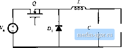 Fig. 3.32 Nonideal hock converter, Problem 3.5. 3.5 In the buck convener of Fig. 3.32, the MOSFET has on-resislante and the diiide forward vnhage drop tan be modeled by a consiam voltage source t . All other losses tan be neglected. (a) Derive a complete equivalent tirctiit model for Ihi s converter. (b) Solve your model to find the oulpui voltage V. (c) Derive an expression for ihe efficiency. Manipulate your expression into a form similar lo Eq. (3.35). 3.S To reduce the switching harmonics present in the input current ofaceruin buck convener, an inptil filter is added as shown in Fig. 3.33. Inductors L[ and contain winding resistances and Sj fespee-tively. The MOSFET ha.s un-resistance and the diode lorward voltage drop can be modeled by a constant vtdlage Vy plus a resistor All other losses can be ignored. 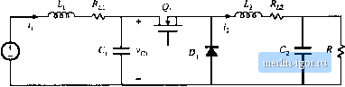 Fig. 3.33 Buck convener with input filter, Problem 3,6. Derive a complete ecuivalenL circuit model Itjr this tircLiil. (b) Solve ytjur model U) linJ the dc ouLpul volltige V. (c) Derive iin expression for the efficienty. ManipLLldle yoLir expression into a lorni similtirto Eq. (3.35-). A 1.5 V battery is to be used to power a 5 V, 1 A load. It has been decided lo use a buck-boost converter in this application. A suitable transistor is found with an on-resistance of 35 m£2, and a Scholtky diode is found wilh a forward drop of 0.5 V. The on-resistance of the Schouky ditide may be ignored. The power stage schematic is shown in Fig. 3.34. -1-W- 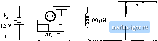 li; 5V < Load = 40 кНг Fig. 3.34 Nonideal buck-boost converter powering a 5 V load from a 1.5 V battery. Problem 3.7 Problems (с) (d) Derive an equivalenl tirtiiit lhal models thede properties of ihis eonverler. IncluJe the iransislur iind Jiode eonJutlioD losses, as well as the inJueliir copper loss, bnl ignore all other sources of kiss. Your moJel shuLild correcdy describe the converter Jc input port. Il is Jesired thai the converter operate with at least 70% efliciency under nominal conJilions (i.e., when the inpiiL voltage i.s 1.5 V and the oulpiil is 5 V al 1 A). How large can the inJuclor winding resistance be? At what July cycle will the converter then operate?/Voff: there is an easy way and a not-so-easy way lo analylically solve this part. For your design ofpart (h), compute the power loss in each element. Plot [he converter outpLLl voltage and efficiency over the range 0 < 1) < 1, using [he value of inductor winding resistance which you selected in part (b). Discuss your pkn t)f part (d). Does it behave as you expect? Explain. For Problems 3.S and a transistor having an on-resislance of (),S ii is used. To simplify the problems, you may neglect all losses other than the transistor conduction loss. You may also neglect the dependence of MOSFET on-resisLance on raleJ blocking voltage. These simplifying assumptions reJuce the differences between converters, but do not change the conclusions regarding which convener performs best in the given situations. 3.8 h is desire J lo interface a 500 V Jc sotnce lo а4(Ю V, 10 A loaJ using a dc-dc converter. Two possible approaches, using buck and buck-boost converters, are illuslrateJ in Fig. 3.35. Use the assumptions described above to: (л) Derive etuivalenl circuit models for both converters, which model the converter input and output ports as well as the transistor conduction loss. Delermine the duly cycles that cause Ihe converters to operate with the specified conditions. Compare the transistor conJuclion losses and efficiencies of Ihe two approaches, and Conclude which converter is better suited lo the specified applitalion. 500 v 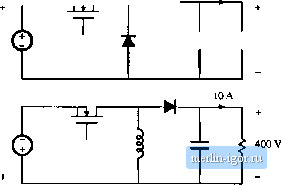 500 v Fig, 3JS Problem 3.S: interfacing a 500 V source to a 400 V load, using (a) a buck convener, (b) a buck-boost converter 3.9 It is desired to interface a 300 V battery lo a 400 V, 10 A load using a dc-dc converter. Two possible approaches, using btjosl and buck-boost converters, are illustrated in Fig. 3.36. Using the assumptions described above (before Problem 3.8), determine the efficiency and power loss of each approach. Which converter is better for this application? 10 A 300V 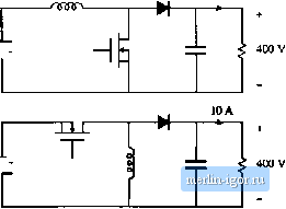 300V - Fig. 3.36 Problem 3.9: intertViciiig a 300 V battery to ti 400 V bad, using: (u) a boost tunverter, (b) a buck-lioost coiivettei. 3.10 A buck ctJDverter h operated frtim the reelified 230 V at mains, such that the converter dc inptil voltage in = 325 V ± 20% A control circuit lulomatically adjusts the converter duly Cycle D, to maintain a constant dc oulpiil voltage t)f V = 240 V dc. The dc Itjad current / can vary over a 10:1 range: 10Л S/< 1 A The MOSFET has an on-resi.4lance оГ U.8 li.The diode condticiion loss can be modeled by a 0.7 V source in series with a 0.2 Q resistor, All other losses can be neglected. (a) Derive an equivalent circuit that models ihe converter input and tiulpiu ports, as vell as the loss elements described above. (ll) Given the range of variation of and / desciibed above, over what range will the duty cycle vary? (c) Al what operating point {i.e., al what value of Vj, and is the converter power loss the largest? What is the value of the efficiency at this opetaung point? 3.11 In the tuk converter of Ftg. 3,37, the MOSFET has on-reststance Л and the diode has a constant forward vohage drop Vf,. All other losses can be neglected. 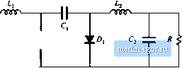 Fig. 3.37 Cuk Cfinverler, Problem 3,1 i. (a) Derive an equivaleni circuit model for this converter. Suggestion: if you dont know how to handle some of the terms in your dc equatitjns, then temporarily leave them as dependent sources. A ttlOre physical representation of these terms may become apparent once dc transformers are incorporated into the model, |