
|
| |
|
Строительный блокнот Introduction to electronics increased to close to 90°. With a small inductance, the controlled rectifier can also operate in discontinuous conduction mode, with modified output voltage chiuacteristics. 17.3.1 Inverter Mode If the dc load is capable of supplying power, then it is possible for the direction of power flow to reverse. For example, consider the three-phase controlled rectifier circuit of Fig. 17.14. The resistive load is repliiced by a voltage source and thevenin-equivalent resistance, capable of either supplying or ctmsum-ing power. The dc load power is equal to Vl, which is positive (rectifier mode) when both Vand are positive. The thyristor is a unidirectional-current switch, which cannot conduct negative current, and hence must always be positive. However, it is possible to cause the output voltage V to be negative, by increasing the delay angle a. The dc load power VI then becomes a negative quantity (inverter mode), meaning that power Hows from the dc load into the 30ac system. Provided that the dc-side filter inductance L is sufficiently large, then Eq. (17.7) is vahd even when the delay angle t:t is greater than 90°. It can be seen in Fig. 17.13 that the dc output voltage V becomes negative f[)r a > 90% iuid hence the power flow indeed reverses. Delay angles approaching 180° iire possible, with the maximum angle limited by commutation ofthe thyristor devices. 17.3.2 Harmonics and Power Factor Let us next consider the hiumonic content and power factor of the phase-controlled rectifier with large inductance. Conipari.son ofthe line current waveform of Fig. 17.12 with that ofthe uncontrolled rectifier (Fig. 17.8) reveals that the waveshapes are identical. The only difference is the phase lag a present in the phase-controlled rectifier. This has the effect of shifting the fundamental component of current (and the harmonicsas well) by angle . The Fourier series is therefore (J-.S) Hence the harmonic amplitudes are the same (the fifth harmonic amplitude is 20% ofthe fundamental, etc.), the THD is again 31%, and the distortion factor is again 95.5%. But there is phase lag in the fundamental component of current, which leads to a displacement factor of cos (a). The power factor is therefore ЛЛ/-1 Fig. 17,14 If the load is capable of supplying power, then the 3( bridge circuit functions as an inverter for V< 0 and re > 90°, Fig. 17.IS Fundamental comimiieiuccinipfex power diagram for the 3(f bridge eirKuit operating in lectifier mode. IIS II sin a
ISII COS a power factor = 0.955 cos (a) (179) which can be quite low when the dc output voltage Vis low. It is at first somewhat puzzling that the introduction of phase control can cause the fundamental current to lag the voltage. Apparently, the rectifier consumes reactive power equal to sm ct (17,10) We normally associate lagging current and the consumption of reactive power with inductive energy storage. But this is not what is happening in the rectifter; indeed, the inductor and capacitor can be removed entirely from the rectifier circuit, and a lagging fundamental current is still obtained by phase control. It is simply the delay of the switching of the rectifiers that causes the current to lag, and no energy storage is involved. So two mechanisms cause the phase-controlled rectifier to operate with low power factor the lagging fundamental component of current, and the generation of current harmonics. Equation (17,10) can be further interpreted. Note that the dc output power P is equal to the dc inductor current / times the dc output voitage V. By use ofEq, (17.7), this can be written , cos u (17.11) Comparison of Eqs. (17.10) and (17.11) reveals that the rectifier fundamental volt-amperes can be expressed using the conventional concepts of complex power = P -I- jQ, where P is the real (average) power consumed and Q is the fundamental reactive power consumed. The complex power phasor diagram, treating the fundamental components only, is illustrated in Fig. 17.15. 17.3.3 Cummutatlon Lets consider next what happens during the switching transitions. In the phase-controlled rectifier circuit of Fig. 17.16, tlie dc-side inductor is large in value, such that its current ripple is negligible. Inductors i- . Lj,. and L, are also present in the ac lines; these may be physical inductors of the rectifier circuit, or they may represent the source impedance of the power systetn, typiciJly the leakage inductances of a nearby transformer. These inductors are relatively small in value. Consider the switching transition iliustrated in Fig. 17.17. Thyristors Qj and Qj initialiycon-duct. At time ( , thyristor is gated on, and the dc current begins to shift from 63 to (Э, The ac line currents ij.t) and if) cannot be discontinuous, since inductors and are present in the lines. So dur- ТПЛГ ТЛПП- v (О i{q, ifQ2 iCq, ТПЛГ Fig. 17.16 Controlled 3(t rectifier circuit, with small ac-side Inductances. ing the interval<t<l.2, thyristors and both conduct, and the voltage V / is zero. Voltage is applied across inductors and L, causing their currents to change; for successful commutation, stiffi-cient volt-seconds must be applied to cause the currents to change from/ to zero, and vice versa. Any stored charge that remains in thyristor (j when current reaches zero must also be removed, and hence i ) actually continues negative as discussed in Chapter 4, When the reverse recovery process of is complete, then is finally in the off-state, and the next subinterval begins with the conduction of thyristors d and Q. The commutation process described above has several effects on the converter behavior. First, it can be seen that the thyristor bridge dc-side voltage vj.1) is reduced in value during the commutation interval. Hence, its average value {v) and the dc output voltage Vate reduced. The amount of reduction is dependent on the dc load current: a liirger dc load current leads to a longer ctjmniutatioii interval, and hence to a greater reduction in (vj). So the rectifier has an effective output resistance. Second, the maxt-mum value ofthe delay angle a js limtted to some value less than 181Г. If a exceeds this limit, then insufficient volt-seconds are available tochange indtictor ctirrent (,(0 from to zero, leading to commutation failure. Third, when the rectifier ac-side inductors are small or zero, so that Z ij and represent Fig. 17,17 Switching transition wavefomis, for the rectifier of Fig. 17.16. Conducting i thyristors: i 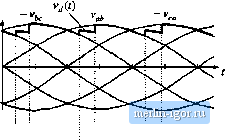 Gt iQt Oil \Qb \ i. I |
|||||||||||||||||