
|
| |
|
Строительный блокнот Introduction to electronics Fig, 4,2 Buck converter: (a) coniaining SPDT switch, {b> containing two SPST switches. /ТППГ с dp R < V 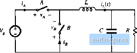 on slate cuirem  most conduct in the on state, For example, in the dc-dc buck converter of Fig, 4.2(b), switch A must block positive voltage when in the off state, and must conduct positive current i when in the on state. If, for all intended converter operating points, the current and blocking voltage lie in a single quadrant of the plane as illustrated in Fig. 4.3, then the switch can be implemented in a simple manner using a transistor or a diode. Use of single-quadrant switches is common in dc-dc cttnverters. Their operation is discussed briefly here. In inverter circuits, two-quadrant switches arc required. The output current is ac, and hence is sometimes positive and sometimes negative. If this current flows through the switch, then its current is ac, and the semiconductor switch realization is more complicated. A two-quadrant SPST switch can be realized using a transistor and diode. The dual case also sometimes occurs, in which the switch current is always positive, but the blocking voltage is ac. This type t)f two-qtiadrant switch can be cttnstructed using a different arrangement of a transistor and diode. Cycloconverters generally require four-quadrant switches, which are capable of blocking ac voltages and conducting ac currents. Realizations of these elements are also discussed in this chapter. Next, the synchronous rectifier is examined. The reverse-conducting capability of the metal oxide semiconductor field-effect transistor (MOSFET) allows it to be used where a diode would normally be required. If the MOSFET on-resistance is sufficiently small, then its conduction loss is less than that obtained using a diode. SynchrontHis rectifiers are sometimes used in low-voltage high-current applications to obtain improved efficiency. Several basic references treating single-, two-, and four-quadrant oflsiat£ voltage Flfi, 4.3 A single-quadraitt switch is capable of conducting currents of a single polarily, and of blocking voltage.s of a single polarity. switches are listed at the end of this eiiapter [1-8]. Several power semiconductor devices are briefly discussed in Section 4.2. Majority-carrier devices, including the MOSFET and Schottky diode, exhibit very fast switching times, and hence are prefened when the off state voltage levels ;ire not too high. Minority-carrier devices, including the bipo-larjnnction transistor (BJT), insulated-gate bipolar transistor (IGBT), and thyristors [gate tnrn-t)ff (GTO) and MOS-contrt)lled thyristor (MCT)] exhibit high breakdown voltages with k)w forward voltage drops, at the expense t)f reduced switching speed. Having realized the switches using semiconductttr devices, switching k)ss can next be discussed. There are a number of mechantsins that cau.se energy to be lost during the switching tr;msttions [11]. When a transistor drives a clamped inductive load, it experiences high instantaneous power loss during the switching transitions. Diode stored charge further increases this loss, during the transistor turn-on transition. Energy stored in certain parasitic capacitances and inductances is lost during switching. Parasitic ringing, which decays before the end of the switching period, also indicates the presence t)f switching los.s. Svvttching lo.ss increases directly with switching frequency, and imposes a maximum limit on the operating frequencies of practical converters. SWITCH APPLICATIONS 4.1.1 Single-Quadrant Switches The ideal SPST switch is illtistrated in Fig. 4.1. The switch contains power terminals 1 and 0, with current and voltage polarities defined as shown. In the on state, the voltage v is zero, while the current / is zero in the off state. There is sometimes a third terminal C, where a control signal is applied. Distingtiish-tng features t)f the SPST switch include the control method (active vs. passive) and the region of the i-v plane in which they can operate. A passive switch does not contain a 1 control terminal C. The state of the switch is determined by the wavefttrms j(r) and v(0 applied to terminals 0 and 1. The most common example is the diode, illustrated in Fig. 4,4. The ideal diode requires that v*) < 0 and > 0. The diode is off (/ = 0) when v < 0, and is on (v = 0) when ( > 0. It can block negative voltage but not po.sitive voltage. A pa.ssive SPST .switch can be realized using a diode provided that the intended operating points [i.e., the values of v(?) and j(r) when the switch is in the on and off states] lie on the diode characteristic of Fig. 4.4(b). The conducting state of an active switch is determined by the signal applied to the control terminal C, The state does not directly depend oti die waveforms v(i) and !(r) applied to terminals 0 and 1. The BJT, MOSFET, IGBT, GTO, and MCT are examples of active swdtches. Idealized characteristics ;(/) vs. i(r) for the BIT and IGBT are sketched in Fig, 4.5, When the control terminal causes the transistor to be in the off state, / = 0 and the device is capable of blocking positive voltage: v >. 0. When the control terminal causes the transistor to he in the ttn state, V = 0 and the device is capable of conducting positive current: I > 0, The reverse-conducting and Fig, 4.4 Diode symbol (a), and its ideal characteristic (b). Fig. 4.5 BipoJni junclion transistor (DJT) and insulated gate bipolui triinsiscoi- (IGBT) symbols (a), and their idealired switch cliaracteii sties (b). rig. 4.6 Power MOSFET symbol (a), and its tdeaiized switch characteristics (b). \ Off V reverse-blocking characteristics of the BJT and IGBT arc poor or nonexistent, and have essentially no application tti the power converter area. The power MOSFET (Fig. 4.6) has sitnilai characteristics, except that it is able to conduct current in the reverse direction. With one notable exception (the synchronous rectifier discussed later), the MOSFET is normally operated with / > 0, in the same manner as the BJT and IGBT. So an active SPST switch can be realized using a BJT, IGBT, or MOSFET, provided that the intended operating potttts lie on the transistor characteristic of Fig. 4.5(b). To determine how to implement an SPST switch using a transistor or diode, one compares the Switch operating points with the i-v characteristics of Figs. 4.4(b), 4.5(b), and 4.6(b). For example, when it is intended that the SPOT switch of Fig. 4.2(a) be in position 1, SPST switch A of Fig. 4.2(b) is closed, and SPST switch В is opened. Switch A then conducts the positive inductor current, j, = and switch В must block negative voltage, i =-V,. The.se switch ttperattng points are tlliistrated in Fig. 4.7. Likewise, when it is intended that the SPDT switch of Fig. 4.2(a) be in position 2, then SPST switch A is opened and switch В is closed. Switch В then conducts the positive inductor current, iy = i/, while switch A blocks positive voltage, l = V. By comparison of the switch A operating points of Fig. 4.7(a) with Figs. 4.5(b) and 4.й(Ь), it can be .ЧССП that a trnnsi.stor (BJT, IGBT, or MOSFET) could be itscd, .since .witch A must block positive voltage and conduct positive current. Likewise, comparison of Fig. 4.7(b) with Fig. 4.4(b) reveals that switch S can be implemented using a diode, since switch В must block negative voltage and conduct positive current. Hetice a valid switch realization is given in Fig. 4.K. |