
|
| |
|
Строительный блокнот Introduction to electronics EMlfitter Boost converter 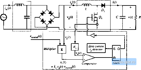 ContrvilcT Fig. 18.20 A typical impicincnialitin of critical conduction inwle control. interval of length / .ТЬе resulting inductor current wavefortn will have a peak value that depends directly on the applied input voltage, and whose average value is one-half of its peak. With either control approach, the converter naturally exhibits loss-free-resistor or ideal rectifier behavior. The emulated resistance is (18.62) This scheme has the advantage of small inductor size and low-cost control ICs. Disadvantages are increased peak currents, variable switching frequency, and the need for additional input EMI filtering. A typical critical conduction mode controller is illustrated in Fig. 18.20. A zero-current detector senses when the inductorcurrent i.s zero; this is typically accomplished by monitoring the voltage acros.s the inductor. The zero-current detector sets a latch, turning on the transistor and initiating the switching period. The transistor current is also monitored, and is compared to a sinusoidal reference vf) that is proportional to the applied input voltage v{t). When the sensed cttrrent is equal to the reference, the latch is reset and the transistor is turned off. Since the switching frequency can vary, possibly over a wide range, it is important to carefully design the converter power stage. For a given power Л the required transistoron-time (, ,can be found by combining Eqs. (18,17) and (IS.62), and solving for/ : , 4LP (18.63) Application of the principle of volt-second balance to inductor L of Fig. 18.20 leads to the following equation: .-v]t. -( (IR.M) Hence, the transistor off-time is given by The switching period V, is equal to t -t >fti,r SubsliUilion oi Etjs. (18.63) and (18.65) into Eq. (18.66) yields r .ALP L vit) (13.65) (18.56) (18.67) The following expression for switching frequency is found by substitution of Eq. (18.11) into Eq. (18.67): l--sin( ) The maximum switching frequency occurs when sill((i)f) equals zero: (18.68) m.x. The minimum sw itching frequency occurs at the peak ofthe sine wave: (18.69) (1S.70) Equations (18.69) and (18.70) can be used to select the value ofthe inductance L and the output voltage V, so that the switching frequency varies over an acceptable range. 18.3.4 NonJintar Carritr Control The nonlinear-carrier controller (NLC) is capable of attaining input resistor emulation in boost and other converters that operate in the continuous conduction mode. Implementation ofthe controller is quite simple, with no need for sensing ofthe input voltage or input current. There is also no need for a cunrent loop error amplifier. The boost nonlinear-carrier charge controller is inherently stable and is free from the stability probietns that require ttddition of an artificial ramp in ciiiTent programmed controllers. A CCM boost rectifier system with nonlinear-carrier charge control is illustrated in Fig. 18.21, and waveforms are given in Fig. 18.22. The reasoning behind this approach is as follows, it is desirable lo conlrol ihe transistor switch current /,.(/), This pulsating current is much easier to sense than the continuous converter input current-a simple current transformer can be used, as in Fig. 18.2]. Further, it is desirable to control the integral of this current, or the charge, for two retisons: (1) integration of the waveform leads to improved noise immunity, and (2) the integral of the waveform is directly related lo its average value. Boost convener 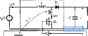 - v,(0 + -e - Ij/n jj Comparator Nonlinear carrier generator (0 < R Latch R 0 S О 0 T, Nonlinear-carrier charge cotitroller Fig. 18.21 Nonlinear-cunier tliarge control i)f u boost conveiter. Fig. 1Й.22 TranKJstor current l(i), paraholit; carrier vultage v (/), and ititcgrator vtiltago Vj(t) ivaveforms for the NLC-coiiti-oHed boost rectifier of Fig. 18.21. |