 | |
|
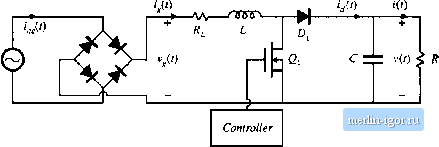
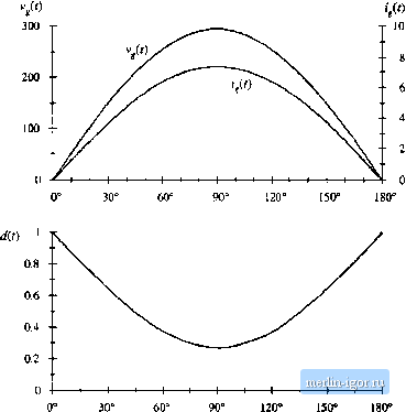
Строительный блокнот Introduction to electronics 18.6 Modeling Losses and Efficiency in CCM Higit-Qmlity Rectifiers 679  -V-ЛЛ (.Large) d=. R<v(t)=V Fig, 18.33 Ac-dc btmsl icctiticr, (a), and a !n*-frequcncy cqLiivuiciit circuit, (b), that models converter losses and efficiency. To find the reclifier waveforms, losses, aud efficiency, we musl solve Ihe circuit of Fig. 18.33(b), under ihe condilions that the conlroller varies ihe duty cycle d(t) such that Et]. (18.124) is satis-lieJ. This leads to time-varying circuit elemenls d(t)R, , an J the (/): 1 iranslormer. The solulion thai follows involves Ihe following steps; (1) solve lor Ihe d(t) waveform; (2) average/ (/) lo find its dc component, equal to the load current /; and (3) find oiher quantities of interesi such as the rectifier efficiency. The simplified boost converler circuit modd of Fig. 18.35, in which only ihe MOSFET conduction loss is accounted for, is solved here. However, the results can be generalized directly to the circuit of Fig. 18.33(b); doing so is left as a homework problem. A similar procedure can also be followed to derive expressions forthe losses and efficiencies of other rectifier topologies. 18.6.1 Expression for Controller Duty Cycle rf(0 The controller varies the duty cycle d(t} such that Eq. (18.124) is satisfied. By solving the input-side loop of Fig. 18.35, we obtain i(t]d(i]R, vJt}-(ru)v Subslilute Eq. (18.124) into (18.125) to ehminate i,((): (IS. 125) i/(Ofi = v,(t)-/(/)v (18.126)   180° Fifi. 18.34 Typical low-fi-cciic(icy components of the boost rectifier wavefortns. with Vj.O) = V sin(o/ We can now solve for the dtity cycle d{t). The result is (18.127} -ЛЛг- dtU): I 1*0) = / AO с . {Large) R<v(t)=V Fig. 18.3S Simplified boost power stage low-frequency equivalem circuit, in which only the MOSFET on-resis-timce is modeled. (18.128) This expression neglects the converter dynamics, an assumption that isjustified when these dynamics are sufficiently faster than the ac line voltage variation. The expression also neglects operation in the discontinuous conduction mode near the zero-crossing ofthe ac line voltage waveform. This isjustified when the rectifier operates in the continuous condttction niode for most of Ihe ac hne cycle, because the power loss near the zero-crossing is negligible. 18.6.2 Expression fur the DC Load Current By charge balance on output capacitor C, the dc load current / is equal to the dc component ofthe diode = Wr . Solution of Fig. 18.35 for yields (18.129) (18.130) From Eq. (18.128), d(t) = 1 - d(t) is given by v-v,(0 (18.131) vlit) v-v,(0 (18,132) |