
|
| |
|
Строительный блокнот Introduction to electronics R < (0.077) R, = (0.077) (27.4 Q) = 2.11 ii (18.147) Of course, other cotiverter losses have tiot beeti accounted for, which will reduce the efficiency. It is instrttctive to compare this result with that obtained tising the expressions for rms current from Section 18.5. The ms uansistor current oflhe ideal CCM btX)St converter is given by liq. (18.119). The rms input cttrrent will be etittai to P.JV = (526 W)/(120 V) = 4.38 A. Hence, Etj. (18.119) predicts an rms transistor ctinent of Ql a. - UicmsSJ у .л IK л. /, 8 (120 V) VI (18.148) = (4,38 A) = 3.48 Л Hence, the MOSFET on-resistance should be chosen according to <.(326W)450OW) 3 !l (4.38 A) This calculadon is approximate because Eq. (18.119) was derived using the wavefonns of the ideal (toss-less) converter. Nonetheless, it gives an answer that is very close to the more exact result ofEq. (18.147). We would expect this approximate approach to exhibit gotxl accuracy in this example, because of the high 95% efficiency. 18.7 IDEAL THREE-PHASE RECTIFIERS The single-phase ideal rectifier concepts of the previous sections can be generalized to cover ideal three-phase rectifiers. Figure 18.38(a) illustrates the properties of an ideal three-phase rectifier, which presents a balanced resistive load to the utility system. A three-phase converter system is controlled such that resistor emulation is obtained in each input phase. The rectifier three-phase input port can then be modeled by per-phase effective resistances R, as illustrated in Fig. 18.38(a). The instantaneous powers apparently constimed by these resistors are uansfetred to the rectifier dc output port. The rectifier output port can thetefore be modeled by power sources etitia! to the instantaneou. ; powers flowing into the effective resistances R. It is irrelevant whether the three power sources are connected in series or in parallel; in either event, they can be combined into a single source equal to the total three-phase instantaneous input power as illustrated in Fig. 18.38(b). If the three-phase ac input voltages are - sin [tut) vj (0 = Vm sin (ш; - 120°) (18.150) vJi) = V sin(u]t-240) dien the instantaneous powers flowing into the phase , h, and с effective resistances R are
1 - cos [201/] (1S.151) Each instantaneous phase power contains a dc term Vl,/(2R,.), and a second-harmonic term. The total instantaneous three-phase power is (1H.I52) This is the instantaneous power which flows out of the rectifier dc output port. Note that the second harmonic terms add to zero, such that the reciifier instanianeous outpui power is constant. This is a consequence of the fact thai the instanianeous power tlow in any balanced three-phase ac system is constant. So, unlike the single-phase case, the ideal three-phase rectifiercan supply constant instantaneous power to adc load, without the need for internal low-frequency energy storage. dc output 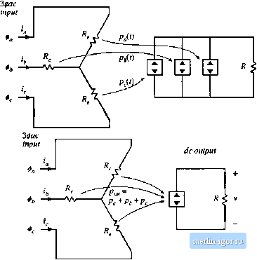 Fig. 1Я.38 development of tlie ideal (hicu-phiiso ruclitier mudol: (a) three ideal single-pha.sc leoiifiers, (h) combination of the three power sources into an equivalent siiigle power stance. input ДО i 1 *о - -ТПЛГ-+ 0. -►-ПЛПГ!-1 до 1Й /*.7 Ideal Tiiree-Fiiase Reaifiers 687 (fc ouiput Fig. 18.39 Riiost-type 30ai;-(lc PWM rectitier. A variety of 30ac-dc PWM rectifiers are ktiowti; a few of the many references on this subject are listed in Ihe references [42-59]. The most well-known topology is the three-phase ac-dc boost rectifier, illustrated in Fig. 18.39. This converter requires six SPST current-bidirectional two-quadrant switches. The inductors and capacitor filter the high-frequency switching harmonics, and have little influence on the low-frequency ae components of the waveforms. The switches of each phase are con-Uoiied to obtain input resistor emulation, either with a multiplying controller scheme similar to Fig. 18.5. or with some other approach. To obtain undistorted line cutrent waveforms, the dc output voltage V must be greater than or equal to the peak line-to-line ac input voltage V. In a typical realization, V is somewhat greater than Vj. This converter resembles the voltage-source inverter, discussed briefly in Chapter 4, except that the converter is operated as a rectifier, and the converter inpul currents aie controlled via high-freqttency pulse-width modulation. The tliree-phase boost rectifier of Fig. 18.39 has several attributes thai make it the leading candidate for most 30ac-dc rectifier applications. The ac input currents are nonpulsating, and hence very little additional input EMI filtering is required. As in the case of the single-phase boost rectifier, the rms transistor currents and also Ihe condttction losses of the three-phase boost rectifier are low relative to other 30ac-dc topologies such as the currenl-source inverter. The converter is capable of bidirectional power flow. A disadvantage is the requirement for six active devices: when compared with a dc-dc converter of similar ratings, the active semiconductor utilization (discussed in Chapter 6) is low. Also, since the reclifier has a boost characteristic, it is not suitable for direct replacement of traditional buck-type phase-controlled rectifiers. The literature coniains a wide variety of schemes for controlling the switches of a six-swilch three-phase bridge neiwork. which are applicable for control of the switches of Fig. 18.39. The basic operation of the converter can be most easily understood by assuming that the switches ate controlled via simple sinusoidal pulse-width modulation. Transistor is driven with duty cycle d(t), while transistor is driven by the complement of d{t), or rf,(t) = 1 - d,(.t). Transistors and Qj are driven with duty cycles djit) and dit), respectively, and transistors Q-,and are driven with duty cycles dU) and d/CO. respectively. The switch volte waveforms of Fig. 18.40 are obtained. The average switch voltages are |