
|
| |
|
Строительный блокнот Introduction to electronics 18.2 Derive expressions for :hc input characteristics of the buck-boost converter, similar to Eqs. (18.25) to (18.33). Sketch the converter input characteristics, and label the CCM-DCM boundary. 18.3 Derive expressions for the tins transistor and diode currents of rectifiers based on the single-phase CCM Cuk topology. Lxptcss your results in forms similar to those of Tabic 18.3. 15.4 To obtain an isolated dc output, the boost converter in Fig. 1S1.5 is replaced by the full-bridge trans-forntcr-isolatcd CCM boost converter of Fig. 6.35. Derive an expression for the rms transistor current. Express your result as a function of/ л, К and V,. 18.5 Comparison of CCM boost and isolated SEPIC topologies as universal-input single-phase rectifiers. You ate given that the dc ouiput voltage is V = 400 V, the load power is f = 500 and the rms itiput voltage varies between 9Q and 270 V, such that the peak ac input voltage V, varies between = 127 V and Maiiu * IJefinc the transistor stress S as the product ofthe worst-case peak transistor voltage and the worst-case rms transistor current, h is desired to minimize S. (a) Determine .V forthe boost convener in this application. (b) Briefly discuss your result ofpart (a): if universal input operation was not required, and hence V = 382 V always, what .5 would result? In the isolated SEPIC, the transformer turns ratio it : 1 can be chosen to optimize the design. (c) Express .V for the SEPIC as a function of n, V, P. д ,i , and V , (d) Choose tl forthe SEPIC such that.? is minimized in this application. Compare with the result.?of parts (a) and (b). 18.6 in the boost-type dc-30ac rectifier of Frg. 18.39, the ac-side inductances L arc not small: they exhibit liitc-frcqucncy iinpcdanccs that should not be ignored. The titrcc-pltasc ac voltages are given by Eq. (18,150), iind the duty cycles arc modulated as in bq. (18,156), fhc converter operates in the continuous conduction mode. (a) Determine the magnitudes and phases of the linc-to-neutral average voltages at the ac inputs to the switch netHork. Express yonr result in terms of D V.and ф, (b) Determine the real power P and reactive power Q drawn from the Зрас .wurcc. Express your results as functions of Vjj, V, D ф, and ujL (c) How must Ф be chosen to obtain unity power factor. 18.7 In the boost-type dc-Зйас rectifier of Fig. 18.39, the switch duty ratios are modulated as illustrated in Fig. 1S1.42. When the inductances L arc sufficiently small, adc output voltage I/equal to the peak line-to-linc ac input voltage can be obtained, with undistorted ac line currents. As illustrated in Fig. 18.42, rf,(r) is equal to 1 for Л°<ш< 60°, where coj = O when {Vi2(f) ) = V. (a) Derive expressions for (/(f) and over theinterval 0° < Crtf £ 60°, (b) State how (/,(f), dU), and should vary over each 60° interval. 18.8 the buck-type 30ac-dc rectifier of Fig. 18.44 operates in fhc continuous conduction mode. Transistors Q, to operate with duty cycles dfi) to (0. respectively. (a) Determine the coiisttaiiits on switch operation. Which transistDrs must not conduct simultaneously? Which duty cycles must total unity? (b) Average the bridge switch network, to detcrntiiic expressions for the average ac-side switch cnn-eiits (/ (г)),- {i))-,;. and {i,(0)i,- (c) Show that the average dc-side switch voltage сш1 be expressed as Ы>) r, = (iC) -ДО) {vjt}) + (rfj(r) - d,(i)] (vM) + {d-,b) - d,{f)) (tv ())r, (d) The duty cycles are varied as follows: 30ac input Input filler Fig, 18,44 Buck-type 30ac-de ifctifief, Froblctn 18,8. dc (juipttt Uwt/ V(()
with tlic ac inptit voltages given by Eq. (18.150). The input filter has negligible effeci of the low-frequency components of the converter waveforms. Determine the steady-state dc output voltage V, as a ftiiictioii of V, l\, and ф. (e) Efcienntnc the power factor. You may assuine that the input filter completely removes the switching harmonics from the cun-ents ( (/), iU). and iit). However, the input fdter elements consume or supply negligible line-frequency reactive power, 18.9 In the three-phttsc DCM flyback rectifter of Fig. 18.45, the hiput Filter htts negligible effect on the low-frequency components of the input ac waveforms. The transistor operates whh switching frequency and duty cycle d. Flyback transformers Tj, Tj.and T, each have magnotiziiig tiiductanee L referred to the primary, tunis ratio n : I, and have negligible leakage inductances. dc ир<и taput filler iTJWv Fig. 18.45 Isolated 30ac-dc rectifier ba.sed on the flyback cotiverter operating in discontinuous conduction mode: Protilein 18.9. (a) Determine expressions for the low-frequency componeiits of the ac input and dc output eurrcnts. (b) Derive an averaged equivalent circuit inodel for tho converter, and give expressions for the eie- Problems ment values. (e) Derive the eonditious for operation in the discotitiuuou.s conduction mode. 18.10 Power stage design of a universal-input boost rectifier. Tlie objective of thi.4 problem is to woik out the power .stage design of a low harmonic rectifier based on the boost conveiter. This conveiter is to be designed to operate anywhere in the world, and hence the input voltage may vary over the range 90 to 270 Vrms, 50 to 60 Hz. The converter produces a regulated 385 V dc otitput, at 1000 W. The .4w-itching frequency/, is 100 kHz. You may assume that the controller operates peifectly, to produce an undistorted ac line cuirent waveform and a well-regnlated dc ontput voltage. (a) Derive an expression for how the duty cycle d(t) will vaty over the ac line cycle. You may neglect converter dynamics and losses. Sketch rf(t) under condition.? of maximum and minimum ac line voltage. (b) Specify the inductor: (i) Specify the value of L such that, at the peak of the sinusoidal input voltage, and under worst-case conditions, the inductor cuiTCiit ripple Ы. is IWc of the instantaneous low frequency current i,(0. (ij) Specify the wor.st-case values of the peak and rms inductor current, assuming 100% efficiency. (c) Determine the worst-case ims currents of the MOSFET and diode, assuming 100% efficiency. (d) Specify the value of С that leads to a worst-case low-frequency (-c/J output voltage peak-peak ripple of 5 V. (e) Given the following loss elements Inductor winding resistance 0.1 ii MOSFET on-resistance 0.4 Ii Diode forward voltage drop 1.5 V Switching loss: model as 1,(0(0.25 Q.) For a constant 1000 W load, and assuming that the controller operates perfectly as described above, find the rectifier efficiency (i) at an ac input voltage of 90 V rms (ti) at an ac input voltage of 270 V rms 18.11 The flyback converter shown in Fig. 18.46 operates iu the continuous conduction mode. The MOSFET I-И- 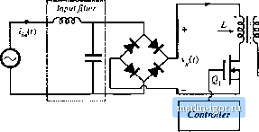 Fig, 18,46 l,ow4tarmonic rectifier sy.stem based on tlie CCM flyback converter, Problem 18.11. has on-resistance K .and diode D, has a constant forward voltage drop Уц. k\\ other loss elements can |