
|
| |
|
Строительный блокнот Introduction to electronics quency is и/, rattier liian Tiie arguments used to model the tank and rectifier/filter networks are imehanged from Section 19.1. The rectifier presents an effective resistive load to the tank, ofvalue R, = ВЛ/тг In consequence, the converter dc conversion ratio is given by 1 = = (19.21) This is a good approximation provided that rtf is close to and that is sufficiently large. Typical characteristics are sketched in Fig. 19.18. The series resonant converter is not generally designed to operate in a subharmonic mode, since the fundamental modes yield greater output voltage and power, and hence higher efficiency. Nonetheless, the system designer should be aware of their existence, because inadvertent operation in these modes can lead to large signal instabilities. 19.2.3 Parallel Resonant DC-DC Converter Example The parallel resonant dc~dc converter is diagrammed in Fig. 19.19. It differs from the series resonant converter in two ways. First, the tank capacitor appears in parallel with the rectifier network rather than in series: this causes the tank transfer function His) to have a different form. Second, the rectifier drives an inductive-input low-pass filter. In consequence, the value of the effective resistance R differs from that of the rectifier with acapacitive filter. Nonetheless, sinusoidal approximations can be used to understand the operation of the parallel resonant converter, As in the series resonant converter, the switch network is controlled to produce a square wave f,(f). If the tank network responds primarily to the fundamental component of i>,(t), then arguments identical to those of Section 19.1 can be used to model the output fundamental components and input dc components of the switch waveforms. The resulting equivalent circuit is identical to Fig. 19.9. The uncontrolled rectifier with inductive filter network can be described using the dual of the arguments of Section 19.1.2. In the parallel resonant converter, the output rectifiers are driven by the nearly sinusoidal tank capacitor voltage l;(t), and the diode rectifiers switch when (0 passes through zero as in Fig. 19.20. If the filter inductor current ripple is small, then in steady-state the filter inductor current is essentially equal to the dc load current /. The rectifier input current ((t) is therefore a square wave of amplitude /, and is in phase with the tank capacitor voltage Vp(f); 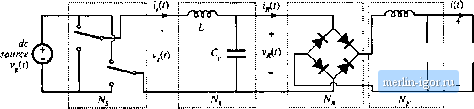 Swildi networii Resonant lanic nerworii Rectifier network Low-pass filter dc nenvorlc load Fig. 19.19 Block diagram uf the parallel resnnant converter fundamental 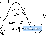 Fig. 1! .2() Rectilier network input terminal wuveforms, fur the parallel resnnant converter; (a) uctaal waveforms v (/) and r((), (b) fundamental coniponents v,(() and 1/(1). =1,1,-1, v/here (p is the phase shift of ICO- The fundamental component of ig{l) is i*a(0 = shi (ш.;-ф ) {19.23) Hence, the rectifier again presents an effective resistive load to the tanlc circuit, etjual to (19.24) The ac components of the rectified tanlt capacitor voltage I Vfflj} I are removed by the output low pass filter. In steady state, the output voltage Vis equal to the dc component of v(() : sill (B,( -фя) (19.25) (14,22) Fiy. 19.21 An ecjuivalent circuit for the rectifier and inductive filter network nf ihe parullel resonant converter, whitb models tbe fundamental components of the rectifier ac Input ftivcforms and the dc components of the load waveforms. So the k)ad voltage V and the tank capacitor voltage amplitude are directly related in steady state. Substitution ofEq. (19.25) and resistive load characteristics V= [R into Et]. (19.24) yields: Л = /г= 1.23Э7Я (19.26) An equivalem circuit for the uncontrolled rectifier with inductive filter network is given in Fig. 19.21. This model is similar to the one used for the series resonant converter. Fig. 19.12, except that the roles ofthe rectifier input voltage v(/) and current if.it) are ititettbanged, and the effective resistance R has a different value. The model for the complete converter is given in Fig. 19.22. Solution of Fig. 19.22 yields the converter dc conversion ratio: Transfer function H(,s) 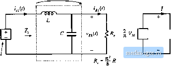 1 $R 21 -- cos (Ф ) 4V Parallel tank network Fig, 19,22 Equivalent cliruit for the p ra?lcl resonant converter, which models the fundamental components of the lank wavefonns, and ttie dc components of the converter input current and output voltage. (19.27) where His) is the tank transferfunction m,s) (19.28) Z (i).vi (19.29) The Bode magnitude diagrams of H(s) and are constructed in Fig. 19.23, using the graphical construction method of Chapter 8. The impedance Zs) is the parallel combination of the impedances of the tank inductor!, capacitor C, and effective load Я.ТЬе magnitude asymptote of the parallel combination of these components, at a given frequency, is equal to the smallest of the individual asymptotes tiiL, 1/юС, and R. Hence, at loW frequency where the inductor impedance dominates the parallel combination, Ij Z(j) II = taZ., while at high frequency the capacitor dominates and Z (j) = 1/tijC, At resonance, the impedances of the inductor and capacitor are equal in tnagnitude but opposite in phase, so that their effects cancel. The impedance Z(i) is then equal to R: +jis>nC- (19.30) with The dc conversion ratio is therefore |
||||||||||||||||||