
|
| |
|
Строительный блокнот Introduction to electronics Fig. 19.23 Construction of Bode diagrams of Zf,s) and H(s) for the pariLe] resonant converter. 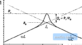 II ЯII (19.31) where FfJ/. At resonance, the conversion ratio is (19.32) The actual pealt value of M occurs at a switching frequency slightly below the resonant frequency, with pealt M slightly greater than Eq. (19.32). Provided that the load resistance R is greater than the tanii characteristic impedance R, the parallel resonant converter can produce conversion ratios both greater than and less than one. In fact, the ideal parallel resonant converter can prtxiuce conversion ratios approaching infinity, provided that the output current is limited to values less than VJR.. Of course, losses limit the tnaxitnum output voltage that can be produced by practical converters. 19.3 SOFT SWITCHINC; As mentioned previously, the soft-switching phenomena Itnown as zero-current switching (ZCS) and zero-voltage switching (ZVS) can lead to reduced switching loss. When the turn-on and/or turn-off Iran- 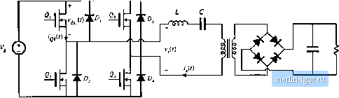 Fig. 19,24 Л serks resonant converter incorporating a full-bridge switch networlt. sitions of a semiconductor switciiing device coincide with the zero crossings of the applied waveforms, some of the switching loss mechanisms discussed in Section 4.3 are eliminated. In converters containing MOSFETs and diodes, zero-voitage switching mitigates the switching loss otherwise caused by diode recovered charge and semiconductor output capacitance. Zero-current switching can mitigate the switching loss caused by current tailing in IGBTs and by stray inductances, Zero-current switching can also be used for commutation of SCRs. In the majority of appUcations, where diode recovered charge and semiconductor output capacitances are the dominant sources of PWM switching loss, zero-voltage switching is preferred. 19.3.1 Operation of the Full Bridge Below Resonance: Zero-Current Switching When the series and parallel resonant inverters and dc-dc converters are operated below resonance, the zero-current switching phenomenon can occur, in which the circuit causes the transistorcurrent to go to zero before the transistor is turned off. Let us consider the operation of the full bridge switch network of the series resonant converter in detail. A full bridge circuit, realized using power MOSFETs and antiparallel diodes, is shown in Fig. 19.24. The switch output voltage v,.(t), and its fundamental component vit), as well as the approximately sinusoidal tank current waveform /,(0, are illnstrated in Fig. 19.25. At frequencies less than the tank resonant frequency, the input impedance of the series resonant tank network Zf{s) is dominated by the tank capacitor impedance [see Fig. 19.1й(а)]. Hence, the tank presents an effective capacitive load to the bridge, and switch current IXO leads the switch voltage fundamental component iviWi as shown in Fig. 19.25. In consequence, the zero crossing of the current waveform occurs before the zero crossing of the voltage !>,.(/).  Conducting devices: Hard S fr Haid Soft vata-imot uim-offuf tum-un of turn-off of 0,.0. Q,.Q, Q.,0> Q Q, Fig, 19,25 Switch rretwork outpui wavefomis for the series resonant conveiter, operated below resonance in the A: = 1 CCM. Zcro-currctit switching aids the transistor titni-olf process. Fig. li .26 Iransisuir Qi vuUage and ctirrent wave-fonriB, for operntien or the series resonani convertei below resonance in the к = 1 CCM. 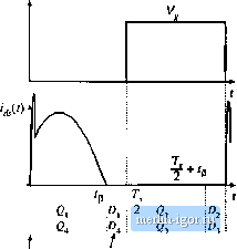 Conducting devices: Hard turn-on Soft tum-ufT ofo,.e ofi? e. For the haif cycle 0 < f < TJ2, the switch voltage v, is equal to + . For 0 < f < fp, the curretit ,(Ois positive and transistors Qj and conduct. Diodes Dj and 0 conduct when f/O is negative, over theinterval l<l < TJ2. The situation during TJ2 <t<T is symmetrical. Since leads v,j(t). the transistors conduct before their respective antiparailel diodes. Note that, at any given time during the condiictioninteival I Ti transistor Qj can be turned off without incurring switching loss. The circuit naturally causes the transistur turn-off transition to be lossless, and long turn-off switching times can be tolerated. 1q general, zero current switching can occur when the resonaat tank presents an effective capacitive load to the switches, so that the switch current zero crossings occur before the switch voltage zero crossings. In the bridge configuration, zero current switching is characterized by the half-bridge conduction .sequence Q-f)j-Q2-D2, such that the transistors are turned off while their respective antiparailel diodes conduct. It is possible, if desired, to replace the transistors with naturally commutated thyii.stors whenever the zero-current-switching property occurs at the turn-off transition. The transistor turn-on transition in Fig. 19.2Й is similar to that of a PWM .switch: it is hard-switched and is not lossless. During the turn-on transition of Q,. diode must turn off. Neither the transistor current nor the transistor voltage is zero. Qj passes thiough a period of high instantaneou.s power dissipation, and switching loss occurs. As in the PWM case, the rever.se recovery current of diode i>2 flows through Q,. This current spike can be the largest component of switching lo.ss. In addition, the energy .stored in the drain-to-source capacitances of and t*; and in the depletion layer capacitance of D is lost when Qj turns on. The.se turn-on tran.sition switching loss mechanisms can be a major disadvantage of zero-current-switching schemes. Since zero-current switching dt>es not addre.ss the switching loss mechanisms that dominate in MOSFET converters, improvements in efficiency ate typically not observed. 19.3.2 (Iperation of the Full Bridge Above Resonance: Zero-Voltage Switching When the series resonant converter is operated above resonance, the zero-voltage switching phenomenon can occur, in which the circuit causes the transistor voltase to become zero before the controller turns the |
||||||||||||||||||