
|
| |
Строительный блокнот Introduction to electronics 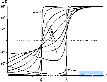 -90J
Hg. 19.JS ZCS/ZVS boiindaiy. LCC inverter example: (a) variatioit ttf tank network input impedaiKe phase shifl with load resistance, (b) Comparison оГД with matchtddoati impedance [. Use ofEq. (19.58) to eliminate Z, from Eq. (19.57) leads to zl< ((9.59) This is tlie desired result. Thequantity Z is the inverter output impedanee, and Й = eonesponds to operation at matched load with maximum output power. The impedances Z,- and Zj, aie purely imaginary, atid hence Eq. (19.59) has nt) real stilutitm unle.ss Z and Z are [)foppo.site phase. As illustrated in Fig. 19.37, if at a given frequency Z and Zjq are both inductive, then zero-voltage switching occurs for all loads. Zero-current switching occurs for all loads when Z- and Z-j, iire both capacitive. Therefore, Theorem 2 is proved. Figure 19.38(ii) illustrates the phase response of Z/jm) as R varies from 0 to for the LCC inverter. A typiciil dependence of Л., and the matched-load impedance Z ottm frequency is illustriited in Fig. 19.38(b). Zero-voitiige switching occurs for all loads when / >/ , imd zero-current switching occurs for all loads when /</o. Over the range/ц < f<f , Z;o is inductive while Z.is ciipiicitive; hence, zero-voitage switching occurs for R < Д.;, while zero-current switching occurs for R > /f,-,. At frequency /m crii = ii il hence the ZVS/ZCS boundary is encountered exactiy at matched loiid. It is commonly desired to obtain zero-voitiige switching at matched load, with low circulating currents and gtKxl efficiency at light loiid. It is apparent that this requires operation in the range/g </</ ,. Zero-voitage switching will then be obtained under matched-ioiid and short-circuit conditions, but will be lost at light load. The choice of element values such that Zq -s: Z is iidvantageous in that the range of loads leading to zero-voitage switching is maximized. 19.4.4 Another Example As a final example, let us consider selection ofthe resonant tank elements to obtain a given output characteristic iU a certain switching frequency, iind lets eviduate the effect of this choice onfi.,;. It is desired to operate a resonant inverter at switching frequency /, = 100 kHz, with an input voltage of = 160 V. The ct)nverter should be capable of producing an open-circuit peak output voitiige 1. = 4(X) V, and should also produce a nominal tiutput [)f 150 Vrms at 25 W. tt is desired to select resonant tank elements thiit accomplish this. Tbe specificiitions imply that the converter should exhibit an open-circuit transfer function of , , V (400 V) \Hjj)\ = j\--f=l,96 (19,60) The required short-circuit current is found by solving Eq. (19.42) tbr l.. vT (19.61) The specifications also imply that the peak voltage and current at the nominal operating point are Substitution of Eq. (19.62) itUo Eq. (19.61) yields [0.236 a1 212 v = 0.27SA 1400 v IVIiitclied load therefore oteurs at the operating point (19,63) (19.63) К. = - = 283У и, = ; = 0.27ЛА Z,(M)=y=l 9Q (19,64) Let us select the values of the tatik elements in the LCC tatik network illustrated in Fig. 19.39(a). The impedances of the .series and parallel branches can be represented using the reactances X. and illustrated in Fig. 19.39(b), with (U,C, The transfer function HJJdiJ is given by the vohage divider formtila The output impedance Zjijtii) is given by the parallel combination (19.65) (19.66) ТППГ Fig. 19.39 Tnk network of the LCC inverter example; (a) schematic, (b) repre.4etttatioti of series and parallel branches by reactances X. and X, |