
|
| |
|
Строительный блокнот Introduction to electronics 4.1 Switch Ajijilicatioiii Sdc input 30(K output 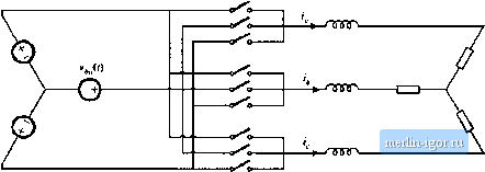 Fig. 4.21 A 30ac-3(iac matrix converter, which requires nine SPST four-quadrant switches, quency and voltage, froin a givea three-phase ae input. Note that there are no dc signals in tltis converter: all of the input and output voltages and currents are ac, and hence four-quadraut switches are necessary. 4.1.5 Synchronous Rectifiers The ability of the MOSFET channel to conduct current in the reverse direction makes it possible to employ a MOSFET where a diode would otherwise be required. When the MOSFET is connected as in Fig. 4.22(a) [note that the source and draiit connections are reversed from the connectioits of Fig. 4.6(a)], the characteristics of Fig. 4.22(b) are obtained. The device can utnv block negative voltage and conduct positive current, with properties similar to those t)f the diode in Fig. 4.4. The MOSFET must be controlled such that it operates in the on state when the diode would normally conduct, and in the off state when the dit)de would be reverse-biased. Thus, we could replace the diode in the buck converter of Fig. 4.S with a MOSFET, as in Fig. 4.23. The BJT has also beeit replaced with a MOSFET in the figure. MOSFET !3j is driven with the ctm-plemeitt of the Q control signal. The trend in computer power supplies is reduction of t)utput voltage levels, from 5 V to 3.3 V and lower. As the output voltage is reduced, the dit)de ctmduction loss increases; in consequence, the diode conduction loss is easily the largest source of power loss in a 3.3 V power supply. Unfortunately, the diodejunction contact potetitial limits what can be done to reduce the forward voltage drop of diodes. Schottky diodes having reduced junction potential can be employed; nonetheless, low-voltage power Fig. 4.22 Poiver MOSFliT connected as a synchronous rectifier, (a), and its idealized switch characteristics, (b). С I - i- (reverse ccnduotion) 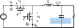 Fijf. 4.23 Blii;!; tonve:ti:i, implemented using л vyriciiromius rcctifici. supplies containing diotJes tliat conduct the outputcurrent must liave low efficiency. A solution is to replace the ditxles witli MOSFETs operated as synchronous rectifiers. The conduction loss of a MOSFET having on-resistance and operated with rms cttrrent is is iy,nR -The on-resistance can be decreased by use of a larger MOSFET. So the conduction loss can be reduced as low ак desired, if one is willing to pay for a sufficiently large device. Synchronous rectifiers find widespread use in low-voltage power supplies. 4.2 Л BRIEF SURVEY OF POWER SEMICONDUCTOR DEVICES The most fundamental challenge in power semiconductor design is obtaining a high breakdown voltage, while maintaining low forward voltage drop and on-resistance. A closely related issue is the longer switching times of high-voltage low-on-resistance devices. The tradeoff between breakdown voltage, on-resistance, and switching times is a key distinguishing feature of the various power devices. The breakdown voltage of a reverse-biased p-n junction and its associated depletion region is a function of doping level: obtainiitg a high breakdown voltage requires low doping concentration, and hence high resistivity, in the material on at least one side of the junction. This high-resistivity region is usually the dominant contributor to the on-resistance of the device, and hence high-voltage devices must have higher on-resistance than low-voltage devices. In majority carrier devices, including the MOSFET and Schottky diode, this accounts for the first-order dependence of on-resistance on rated voltage. However, minority cnmcr devices, including the diffiised-junction p-ii diode, the bipolar junction transistor (BJT), the insitlated-gate bipolar transistor (IGBT), and the tliyristor fainily {SCR, СТО, MCT), exhibit another phenomenon known as conductivity modulanon. When a minority-carrier device operates in the on state, minority carriers are injected into the lightly doped high-resistivity region by the forward-biased /j-H junction. The resulting high concentration of minority carriers effectively reduces the apparent resistivity of the region, reducing the on-resistancc of the device. Hence, minority-carrier devices exhibit lower on-tesistances than coinparable majority-carrier devices. However, the advantage of decreased on-resistance in miitority-carrier devices comes with the disadvantage of decreased switching speed. The conducting state of any semiconduttttf device is controlled by the presence or absence of key charge quantities within the device, and the turn-on and turn-off switching times are equal to the times required to insert or remove this controlling charge. Devices operating with conductivity modulation are controlled by their injected minority carriers. The total amount of controlling minority charge in minority-carrier devices is much greater than the charge required to control an equivalent majority-carrier device. Althoitgh the mechanisms for inserting and removing the controlling charge of the various devices can differ, it is nonetheless true that, because of their large amounts of minority charge, minority-carrier devices exhibit switching times that are significantly longer than those of majority-carrier devices. In consequence, majority-carrier devices find applicatioit at lower volt- age levels and higher switching frequencies, while the reverse is true of minority-carrier devices. Modern pt)wer devices are fabricated using up-to-date processing techniques. The resulting small feature size allows construction of highly interdigitated devices, whose tinwanted parasitic elements are less significant. The resulting devices are more rugged and well-behaved than their predecessors. A detailed description of power semiconductor device physics and switching mechanisins is beyond the sct)pe of this book. Selected references on power semiconductor devices are listed in the reference section [9-19]. 4,2.1 P()wt!r Diodes As discussed above, the diff used-junction р-н diode contains a lightly doped or intrinsic high-resistivity region, which allows a high breakdown voltage It) be obtained. As illustrated in Fig, 4.24(a), this region comprises one side of the /)- junction (denoted )Г); under reverse-biased conditions, essentially all of the applied voltage appears across the depletion region inside the н region. On-state conditions are illustrated in Fig. 4.24(b). Holes are injected across the forward-biased junction, and become minority carriers in the n region. These minority carriers effectively reduce the apparent resistivity of the ii~ region via conductivity modulation. Essentially all t)f the fonvard current ((r) is comprised of holes that diffuse across the p~n region, and then recombine with electrons from the j? region. Typical switching waveforms are illustrated in Fig. 4.25. The familiarexponential j-vcharacter- LiJK doping concuntratiiin © © Fig. 4,24 reverse-bias Power diode: (a) under conditions, (b) under Depletion regim, wverse-biaied forward-hia.s conditions. Cwfu/uitivf/v miKluUaion © i-- О © Minority carrier injection |