
|
| |
Строительный блокнот Introduction to electronics 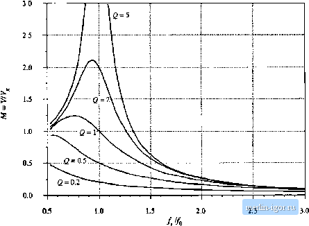 Fig. 19.52 Exact contn)! characteristics of the parallel resonant converter, with о resistive load. Both CCM and DCM operation Is included, for 0.5 <, E 3. M =l-cos(P) cos (а + р)-2со,ч(а) = -1 i(o; + P) + 2sin{ ) + (S-a) = 2y P + 5=Y Af = 1+ U-fil (19.97) Unfortutiately, the solntioti to this set of etjnations is tiot linown iti closed form, because ofthe inixtnre t)f litiearand trigtinoinetric terms. In consequetice, the equatit)tis must be solved iteratively. Fora given Y and J, a coinputer is used to iteratively find the angles (X, P, atid 5. Л/ is then evaluated, atid the output platie characteristics cati be plotted. The result is given in Fig. 19.51. The dashed lines are the DCM st)iutions, and the solid lines are the valid CCM solutions. Figure 19.51 describes the coiuplete dc behavior of the ideal parallel resonant converter for ail switching fretjuencies above 0,5/ц. Ft)r given values of normalized switching frequency F = fjfi - n/y, the relationship between the nonualized output current J and the normalized t)utput voltage M is apprtwimately elliptical. At resonance {F = 1), the CCM ellipse degenerates to the horiztmtal line J= 1, and the converter exhibits current source characteristics. Above resonance, the converter can both step up the voltage (M > 1) and step down the voltage (M < 1). The normalized load current is then restricted to J < 1, corresponding to / < VJnlif,. For a given switching fret]uency greater than the resonant fretjuency, the actual limit on maximum load current is even more restrictive than this limit. Below resonance, the converter can also step up and step down the volt- age. Normalized load eurrenis greater than tme are also obtainable, depending on M and F. However, no solutions occur when Mandiare sinnultaneously large. In Fig. 19.52, (he control plane characlerislics are ploUed for a resisltve load. The parameter Q is defined for the parallel resonant Converter as Q = RlrR, The normalized load current is then given by 7 = WQ. W.fi SUMMARY OF KEY POINTS 1. The sinusoidal approximiilion allows a greiit deal of insight to be gained into the operation of resoniint inverters and dc-dc converters, The voltage conversion radc of dc-dc resonant converters can be directly related to the lank network transfer function. Other important converter properties, such as the output characteristics, dependence {or lack thereof) of transistor Current on load current, and lero-vollage- and zero-Current-switchtng transitions, can also be understood using this approxirnadon. The approximation is at:curate provided thtit the effective Q facttjr is sufficiently brge, tind prtjvided that the switching frequency is sufficienlly close to resonance, 2. Simple equivalent circuits are derived, which represent the fundamental components of the lank network wjveforms, and the dc ctjmponents of the dc terminal waveforms. 3. E?LJCt solutions of the ideal dc-dc series and parallel resonant converters are listed here as well. These solutions correctly predict the conversion ratios, for operation not Only in the fundamental continuous conduction mode, but in discontinuons and subharmonic modes as well. 4. Zero-voltage switching mitigates the switching loss caused by diode recovered charge and semiconductor device output capacitances. When the objective is to minimize switching loss and EMI, it is preferable to operate each MOSFET and diode with zero-voltage switching. 5. Zero-currenl switching leads to natural commutation of SCRs, and can also mitigate the switching loss due. to current [ailing in IGBTs. 6. The input impedance magnitude 7J, and hence idso the transistor current magnitude, are monotonic lunctions ol the load resistance R. The dependence of the transistor conduction loss on the load current can be easilv understood hv simplyplotttng in the limiting cases as /? - < and as/f - 0, orjj and 7. The ZVS/ZCS boundary is also a simple function oJ Zj- and Z, If ZVS occurs at open-circuit and at short-circuit, then ZVS occurs for all loads. If ZVS occurs at short-circuit, and ZCS occurs at open-circuit, then ZVS is obtained at matched load provided that j Z, > Z,j . 8. The output characteristics of all resonant inverters considered here are elliptical, and are described completely by the open-circuit transfer function magnitude [ , and the output impedance 7, . These quantities can he chosen lo malch lhe output characteristics to the applicalion requirements. Reference. [1] F.C. ScHWARZ, An Improved Method of Resonant Current Pulse Modulation for Power Converters, IEEE Power Electronics Specialists Conference, 1975 Record, pp. 194-204, lunc 1975. [2] R.L. SiEtOERW.iLD, High Frequency Resonant Transistor De-De Conveners, IEEE Transactions on Industrial Electronics. Vol. 31, No. 2, pp. lSl-191, May 19Й4. [3] M. Cosby and R. Nelms, Designing a Parallel-Loaded Resonant Invcncr for an Electronic Ballast Using the Fundamenlitl Approximittion, IEEE Applied Power Electronics Conference, 199ji Record, pp. 41323. [4] M. gulko iind S. BEN-Y.4AK0V, CunenL-Sourctng Push-Pull Pariillel-Resoniince Inverter (CS-PPRI): Theory and Applitaliun as ii Fluorescent Lamp Driver, IEEE Applied Power Electronics Conference, 1993 Record, pp. 411-417. [5] Y. Ct[eron, H. FociL, and J. Salesses, SUidy oS a Resonant Converter Using Power Transistors in a 25 kW X-rity Tube Pimei:Su]iply, IEEE Power Elearonics Specialists Conference, Proceedings ESA Sessions, pp. 295-306, June 19S5. [6] S. D. JoiK.wn, A. F. WiTuLSKi, and R. W. Erickson, A Comparison uf Resoaaai Topologies in High Voltage Applications, IEEE Transactions on Аего.1расе and Electronic Sy.ileins, Vol. 24, No. 3, pp. 263-174, July 198S. [7] Y. MuRAi and T. .A. Lipo, High Frequency Series Resonant Dc lank Power Conversion, IEEE Industry Applications Sociery Annual Meeting, 19SS Record, pp. 648-656. [8] F. C. ScuwARZ, A Etoublesided Cyclo-Converler, IEEE Power Electronics Specialists Conference, 1979 Record, pp. 4377. [9] D, d[van, The Resonani Dc Lint Converter: A New Concept in Stntic Power Conversion, IEEE Indus- try Applications Society Annual Meeting, 1986 Record, pp. 648-656. [10] R.L. Steigerwald, A Comparisun of Half-Bridge Resonant Converter Topologies, IEEE Applied Power Electronics Conference. 1987 Record, pp. 135-144. [11) R. Seveens, Toptilogies for Three Element Resonant Converters, IEEE Applied Power Eiecirouics Conference. 1990 Recurd, pp. 712-722. [12] M. KAZlMtERCZUK, W. SZARANIEC, and S. Wang, Analysis and Design of Parallel Resonant Converter at Uih Qi IEEE Tran.tactions on Aero.space a?id Electronic Sy.ttems, Vol. 28, pp. 35-50. January 1992. [П] R. King and T. Stuart, A Normalized Model for the Half Bridge Series Resonant Cunverter, IEEE Transactions on Aerospace and Electronic Sy.itein.i, March 1981. pp. 180-193. [14] V. Vorperian- and S. 6vK, A Complete DC Analysis of [he Series Resonant Converter, IEEE Power Electronics Speciali.ils Conference. 1982 Recurd, pp. 85-100, June 1982. [15] R. KiKG and T.A. SruART, Inherent Overload Protection for the Series Resonant Converter, IEEE Tra/tt-actions onAe/ospacc and Electronic Systems, 19, No. 6, pp. S20-830, Nov. 19S3. [16] A. WiTULSKi and R. Erickson, Steady-State Analysis of the Series Resonant Converter, IEEE Transac-tiotis on Aerospace and Electronic Systems, Vol. 21, No. 6, pp. 791-799, Nov. 19S5. [17] A. WiTULSKt and R. Erickson, Design ol the Series Resonant Converter for Minimum Component Stress, IEEE Transactions on Aerospace and Electronic Systems, Vol. 22, No. 4, July 1986, pp. 356-363. [18] R. ORLGANTt and F.C. Lee, Resonant Power Processors, Part 1: State Plane Analysis, IEEE Transactions on Industry Applicatinn.f, Vol. 21, Nov ./Dec. 1985. pp. 1453-1460. [19] C.Q. Lee and K. SiR[, Analysis and Design of Series Re.sonant Converter by State Plane Diagram, IEEE |