
|
| |
|
Строительный блокнот Introduction to electronics 20.1 Sofi-Swilcking Mechiisnis of Semkoiidtjctor Devices 763 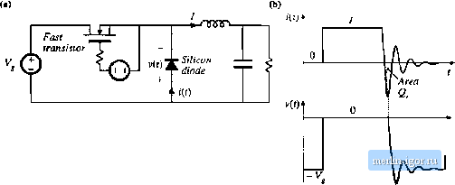 Fig. 20.1 Hard switching at the tum-oFT transition of щ diode, conventional buck converter exatnple: (a) schematic, (b) diode voltage and current waveforms. 20.1.1 Diiide Switching As discussed in Chapter 4, the reverse-recovery process usually leads to significant switching loss associated with the turn-()lT transititm of diodes. This is often the largest single stiurce oi loss in a hard-switched converter. Normally, negligible hm is associated wilh the turn-on transition of pimer diiides. Three types of diode tiu-n-olf transition waveforms are commonly encountered in modern switching converters: hard Switching, zero-current swhching, and zero-voltage switching. Figure 20.1 illuslrales a conventitinal hard-switched PWM buck converter. The diode voltage and current wavelbrms v(/) and /(r) are also illustraled, wilh an exaggerated reverse recovery time. The (lutpul inductor current ripple is small. The ditide turns tilT when the transistor is turned on; the reverse recovery process leads to a negative petik current of large amplitude. The diode must immediately support the full reverse volttige V, Eind hence both v(t) and i(t) must change with large slopes during reverse recovery. As described in Section 4.3.2, hard switching of the diode induces energy loss in the transistor, given approximately by {20.1) where gis the diode recovered charge and (is the reverse recovery time, both taken to be positive quantities. The recovered chtirge is relatively large because the slope di/dt is large during the turn-off transition. The resonant circuii formed by the diode tiulput capacitance Cj and the diode package and other wiring inductances letids to ringing at the end ofthe reverse recovery time. Figure 20.2 illustrates zero-current switching at the turn-olTlransitionofadiode. The converter example is a quasi-resonant zero-voltage switching buck converter (see Section 20.3.1). The outpul inductor current ripple is again small. However, tankinducltir L,. is now ctmnected in series wilh the diode. The resulting ditide current waveform changes with a limited skipe as shown. The diode reverse-recovery process commences when ((f) passes through zero and becomes negative. The negative i{t) actively removes stored charge from the diode; during this reverse recovery time, the diode remains forward-biased. When the stored charge is removed, then the diode voltage must rapidly change to - V. As de.scribed in Section 4.3.3, energy Wjis stored in inductor at the end ofthe reverse recovery dme, given by Soft Swilching ((() Ф T - >iCO  Vlrea i 2. Fig, 20.2 Zero-current switching at tlte turn-otT transition of a diode, ZVS quasi-resonant Ъпск converter example: (a) converter scliematic, (b) diode voltage and current wavefonns. (20.2) The resonant circuit formed by and tlie diode outputcapacitance Cj then cause this energy to be circulated between and t.y. This energy is eventually dissipated by parasitic resistive elements in the circuit, and hence is lost. Since Eqs. (20.1) and (20.2) are similar itt fonn, the switching losses induced by the reverse-recovery processes of diodes operating with hard switching and with zero-current switching are similar in magnitude. Zero-current switching may lead to somewhat lower loss because the reduced di/dt leads to less recovered charge Q. Zero-current switching of diodes also typically leads to increased peak inverse diode voltage during the ringing of and C,., because of the relatively large value of L. When a diode operates with hard switching or zero-current switching, and when substantial inductance is present in series with the diode, then significant ringing is observed in the diode voltage waveform. A resonant circuit, comprised of the series inductance and the diode output capacitance, is excited by the diode reverse recovery process, and the resulting ringing voltage can be of large enough magnitude to lead to breakdowit and failure of the diode. A common example is the diodes on the secondary side of a hard-switched transformer-isolated converter; the resonant circuit is then formed by the transformer leakage inductance and the diode output capacitance. Other examples are the circuits of Figs. 20.2 and 20.36, in which the series inductance is a discrete tank inductor. A simple snubber circuit that is often used to protect the diode from excessive reverse voltage is Fig, 20,3 A dissipative suubber circuit, for protection of a diode from excessive voltage caused by ringing. -nsrsv Series inductance R ЛЛг- Diode output capacitance Snubber circuit Tank circuit Fig. 20,4 Zeru-vdltage switching at the turn-off transition of a diode, ZVS qtjasi-squarewavc buck converter example: (a) converter schematic, (b) diode current and voltage wavefonns. 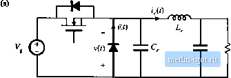
illustrated in Fig. 20.3. Resistor r damps tlie ringing of the resonant circuit. Capacitor с prevents the off-state voltage of the diode from causing excessive power loss in r. Nonetheless, tlie energy consumed by Д per switching period is typically greater than Etjs. (20.1) or (20.2). Figure 20.4 illustrates zero-voltage switching at the turn-off transition of a diode. The figure illustrates the example of a zero-voltage switching quasi-square wave buck converter, discussed in Section 20.3.3. The output inductor of this converter assumes the role ofthe tank inductor, and exhibits large current ripple that causes the current Д() to reverse polarity. While the ditxle conducts, its current !(/) is equal to j(f). When becomes negative, the diode continues to conduct until its stored charge Q,. has been removed. The diode then bectjines reverse-biased, and ifit) flows through capacitor and the diode output capacitance C.. The ditxle voltage and current both change with limited slope in this type of switching, and the loss induced by the ditxle reverse-recovery process is negligible because the waveforms are not significantly damped by parasitic resistances in the circuit, and because the peak currents during rever>ie recovery are relatively low. The diode stored charge and diode output capacitance both behave as an effective nonlinear capacitor that can be combined with (or replace) tank capacitor C. Snubber circuits such as Fig. 20.3 are not necessary when the diode operates with zero-voltage switching. Thus, zero-voltage switching at the turn-off transition of a diode is the preferred approach, that leads to minimum switching loss. Zero-current switching at the turn-off transition can be problematic, because ofthe high peak inverse voltage induced acrtjss the diode by ringing. 20.1.2 MOSFET Switching The switching loss mechanisms typically encountered by a MOSFET in a hard-switched ctmverter are discussed in Chapter 4, and typical MOSFET vtdtage and current wavetbrms are illustrated iu Fig. 20.5. The most significant components of switching loss in the MOSFET of this circuit are: (1) the loss |