
|
| |
|
Строительный блокнот Introduction to electronics Soft Switchitig  Fig. 20.5 Hard switciiing of a MOSFET in a conventionti! buck converter: (a) schematic, (b) MOSFET voltage and curreni waveforms. induced by the diode reverse recovery process, and (2) the loss of the energy stored in the MOSFET output capacitance C . Both loss mechanisms occur during the MOSFET turn-on process. In the hard-switched circuit of Fig. 20.5, there is essentially no switching loss incurred during the MOSFET turn-off transition. This occurs because of the substantial output capacitance Cy, of the MOSFET This capacitance holds the voltage v{i) close to zero while the MOSFET turns off, so that the turn-off switching k)ss is very small. After the MOSFET has turned t)ff, the output indtictor current / flows through Cj,. The voltage v(t) then increasesuntil =V and the diode becomes forward biased. However, when the MOSFET turns on, a high peak current flows through the MOSFET channel, induced by the diode reverse recovery and by the output capacitances of the MOSFET and diode. This leads to substantial energy loss during the hard-switched turn-on transition of the MOSFET. When a MOSFET (or other transistor) operates with hard switching, and when substantial inductance is present in series with the MOSFET, then significant ringing is observed in the MOSFET voltage waveform. A resonant circuit, composed of the MOSFET output capacitance and the series inductance, is excited when the MOSFET turns off, and the resulting ringing vtdtage can be of large enough magnitude to lead to breakdown and failure of the MOSFET. A common example is the MOS- Snubber circuii  Fig, 20.6 Insertion of a dissipative voltage-clainpetl snubber circuit into a ilyback converter. The MOSFfiT voltage is clamped to a peak value of (V + v,.). FET ofthe flybaek eonverter, in whieh series incJuetanee is introdueecJ by the transfornner leakage inductance. An R-C snubber circuit, similar to that used for the dit)de in Fig. 20.3, can be used to protect the MOSFET from damage caused by excessive applied voltage. Another common snubber circuit is illustrated in Fig. 20.6. When the MOSFET turns off, the current flowing in the transforraer leakage inductance begins to flow into the MOSFET capacitance С,д. These parasitic elements then ring, and the peak transistor voltage can significantly exceed the ideal value of {DiD)V. One simple way to design the snubber circtiit of Fig. 20.6 is to choose the capacitance Cj to be large, so that vit) = 1. contains negligible switching ripple. The resistance is then chosen st) that the power consumption of at the desired voltage V, is equal to the switching loss caused by Lf. (20.3) The current / is equal to the current flowing in the transformer primary just before the MOSFET is turned off. This approximate expression is useful for obtaining a first estimate of how to choose to t)btain a given desired V. Zero-current switching does not affect the switching loss that arises from the MOSFET output capacitance, and it may or may not influence the loss induced by diode reverse rectiveiy. In con.sequence, zero-current switching is of little or no help in improving the efficiency of converters that empltiy MOSFETs. Zero-voltage switching can prevent both diode reverse recovery and semiconductor output capacitances from inducing switching loss in MOSFETs. An example is illustrated in Fig. 20.7. This circuit is again a zero-voltage switching qtiasi-squarewave example, discussed in Secrion 20.3.3. The converter circuit naturally discharges the energy stored in C before the MOSFET is switched on. When the drain-to-source voltage v(/) passes through zero, the MOSFET btidy diode becomes forward-biased. The MOSFET can then be turned on at zero voltage, without incurring turn-on switching loss. The MOSFET turn-on transition must be completed beftjre the tank inductor ctirrent i,.(/) bectmes positive. The MOSFET turn-off transition is aist) Itjssless. and is similar to the hard-switched case discussed above. Zero-voltage switching of a MOSFET also causes its body diode to operate with zero-voltage switching. This can eliminate the switching loss associated with reverse recovery of the sltiw btidy diode, and improve the reliability of circuits that forward-bias this dit)de. 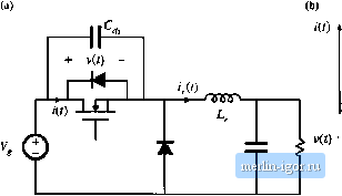
Fig. 20,7 Zero-vohage switching of a MOSFbf, ZVS quasi-squarewave buck converter example. The MO.SFET, its tindy diode, aud its output cupatitance С, are illuitrated, (a) converter schematic, (b) MtJSlET voltage and current waveforms. Zero-voitage switehing ean also eliminate ttie overvoitage problems associated with transformer iealtage inductances, removing the need for voltage-clamped snubber circuits such as in Fig. 20.6. An example is discussed in Section 20.4.2. 2().1.3 1(;BT Switching Like the MOSFET, the IQBT typically encounters substantial switching loss during its turn-on transition, induced by the reverse-recovery process of diodes within the converter. In addition, the IGBT exhibits significant switching loss during its turn-off transition, caused by the current tailing phenomenon (see Chapter 4). Zero-voltage switching has been successfully applied to IGBT circuits-an example is the auxiliary resonant commutation circuit discussed in Section 20.4.3. This has the principal advantage of eliminating the switching k)ss caused by diode reverse recovery. Although zera-voltage switching can reduce the k)ss incurred during the turn-off transition, it is difficult to eliminate the substantial loss caused by current tailing. 20.2 THE ZERO-CURRENT SWITCHING QUASI-RESONANT SWITCH CELL Figure 20.8(a) illustrates a generic buck converter, consisting of a switch cell cascaded by an L-C low-pass filter. When the switch cell is realized as in Fig. 20.8(b), then a conventional PWM buck converter is obtained. Figures 20.8(b) and (c) illustrate two other possible realizations of the switch cell: the half-wave and full-wave zero-current-switching t]uasi-resonant switches [1, 2]. In these switch cells, a resonant tank capacitor C is placed in parallel with diode Dj, while resonant tank capacitor is placed in series with the active transistor element. Both resonant switch cells require a two-quadrant SPST switch. In the half-wave switch cell of Fig. 20.K(c), diode is added in series with transisttw 0- This causes the Qj-D SPST switch to turn off at the first zero crossing of the tank inductor current /i(f)- In the full-wave switch cell of Fig. 20.K(d), antiparallel diode Л, allows bidirectional fk)w of the tank inductor current !(()i With this switch network, the Q-D, SPST switch is normally turned off at the second zero-crossing of the i(0 waveform. In either switch cell, the and elements are relatively small in value, such that their resonant frequency /, is greater than the switching frequency/ where In the analysis which follows, it is assumed that the converter filter element values Land С have negligible switching ripple. Hence, the switch cell terminal waveforms v{t) and yf) are well-approximated by their average values: v,(/)-{v.(i)), with the average defined as in Eq. (7.3). In steady-state, we can further approximate v(t) and /(r) by their dc components V, and |