 | |
Строительный блокнот Introduction to electronics  ТЛПГ1 i(f)
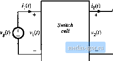
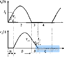
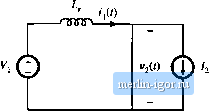
R к y(t) Viit)  Switch network I Half-wave ZCS quasi-resonant switch cell ТЛПГ Switch network \ Full-wave ZCS quasi-resonant switch cell Fig, 20.8 Implementation of the switch cell in a buck converter: (tt) buck converter, witli arbitrary switch cell; (b) PWM switch cell; (c) half-wave ZCS quasi-resonant switch cell; (d) full-wave ZCS quasi-resonant switch cell. Sofi SwUching  Switch tietwork \ Half-wave ZCS quasi-resonant switch cell Fig. 2tt.*t The halt-wave ZCS qiyiisL-retonani twittheeli, driven by tho icvminal (iiiantitie£(v(t))j, and (((f))-j-. (20.6) Thus, the small-ripple approximation is employed for the converter filter elements, as usual. To understand the operation of the half-wave ZCS quasi-iesonant switch cell, we can solve the simplified circuit illustrated in Fig. 2(W. in accordance with the averaged switch inodeling approach of Sections 7.4 and 11.1, it is desired to determine tlte average terminal waveforms (fW)?; and {i{t))j., as functions of the applied quantities (v,(f))-,; and (tjf))?;- switch conversion ratio ft is then given by In steady state, we can write V, I, (20.7) (208) The steady-state analysis of this section employs Eq. (20.S) to determine/i. 20.2.1 Waveforms of the Hall-Wave ZCS Quusi-Resoniint Switch Cell Typical waveforms of the half-wave cell of Fig. 20.9 are illustrated in Fig. 20.10. Each switching period consists of four subintervals as shown, having angular lengths a, p, 5, and t,. The switching period begins when the controller turns on transistor Q,. The initial values of the tanli inductorcurrent ij(r) and tank capacitor voltage vW are zero. During subinterval 1, all three semiconductor devices conduct. Diode is forward-biased because f,(() is less than Ij. In consequence, during subinterval 1 the switch cell reduces to the circuit of Fig. 20.11. The slope oftite inductorcurrent is given by Subitaerval: 1 Fig. 20,ie Tank inductor current arid capacitor voltage waveforms, for the ha If-wave ZCS quasi-res-onantfiwitchofFig, 20.9, ОоГ, - Cotuiuclmg e, Q, X devices:  with the initial randition ii(0) = 0. The solutitm is r,(0.-[it = a)£ (20.10) where the tank characteristic impedance Я,] is defined as R - (20,11) It is convenient to express the waveforms in terms ofthe angle 0 = Ci)(/, instead of time f. At the end of subinterval 1, сОц = Ct. The subinterval ends when diode Dj becomes reverse-biased. Since the dit>de D. current is equal to /j -  |
|||||||||||||||||||||||