
|
| |
|
Строительный блокнот Introduction to electronics Fig. 4.2S Diode voltage and turrcnt waveforms. Interval (1): off state. Interval (2): turn-on transition. Interval (3): on state. Iniervals (4) and (5): lutn-off transition. Interval (6): otf state. 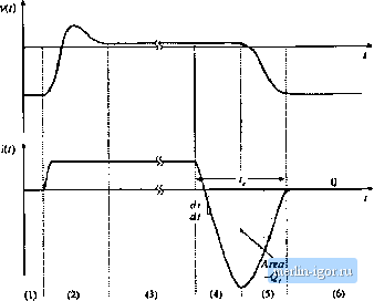 istic of the p-n diocie is an et]iiilibritjm relatit)n. During transients, significant deviations from the exponential characteristic are observed; these deviations are associated with changes in the stored minority charge. As illustrated in Fig. 4.25, the diode operates in the off state during interval (1), with zero current and negative voltage. At the beginning of interval (2), the current increases to some positive value. This current charges the effective capacitance t)f the reverse-biased diode, supplying charge to the depletion regjon and increasing the voltage v(t). Eventually, the voltage becomes positive, and the diode junction becomes forward-biased. The voltage may rise to a peak value of several volts, or even several tens of volts, reflecting the somewhat large resistance of the lightly doped iC region. The forward-biased junction continues to inject minority charge into the n~ region. As the total minority charge in the n regit)n increases, conductivity modtilation t)fthe n~ region causes its effective resistance to decrease, and hence the ft)rward vt)ltage drop \it) also decrea.ses. Eventually, the diode reaches equilibrium, in which the minority carrier injection rate and recombination rate are equal. During interval (3), the diode operates in the on state, with forward voltage drop given by the diode static i-v characteristic. The turn-off transient is initiated at the beginning of interval (4), The diode remains forward-biased while minority charge is present in the vicinity of the diode junction. Reduction of the stored minority charge can be accomplished either by active means, via negative terminal titrrent, or by passive means, via recombination. Normally, both mechanisms occur simultaneously. The charge 2contained in the negative portion of the diode titrn-off current waveform is called the recovered charge. The portion of Qr occurring during interval (4) is actively-removed minority charge. At the end of interval (4), the stored minority charge in the vicinity of the fJ-f) jtmction has been removed, such that the d[t)de junction becomes reverse-biased and is able to block negative voltage. The depletion region effective capacitance is then charged during interval (5) to the negative off-state voltage. The portion of Q, occitrring during interval (5) is charge supplied to the depletit)n region, as well as minority charge that is acdvely retuoved from remote areas of the dit)de. At the end of interval (5), the diode is able to block the entire applied reverse vt)ltage. The length t)f intervals (4) and (5) is called the reverse recover) time t. During interval (6), the diode operates in the off state. The diode turn-off transition, and its inflitence on switching loss in a PWM converter, is discussed further in Section 4.3.2. ТаЫс 4-1 Charat;Len4tics of several eommertjiiil power rectifier dindes
Diodes are rated according to the length of their reverse recovery time f. Standard recovfiy rectifiers are intended for 50 Hz or 60 Hz operation; reverse recovery times of tliese devices are usually not specified. Fast recowry rectifiers and ultrafasT recovery rectifiers are intended for use in converter applications. Tiie reverse recovery time t, and soinetiines ;ilso the recovered cliarge Q, are specified by manufacturers of tliese devices. Ratings t)f several cominercial devices are listed in Table 4.1. Schottky diodes are essentially inajority-carrierdevices whose operation is based on the rectifying characteristic of a nietal-semiconductor junction. These devices exhibit itegligible minority stored charge, and their switching behavior can be adequately inodeled simply by theirdepletion-region capacitance and equilibriuin exponential i-v characteristic. Hence, an advantage of the Schottky dit)de is its fast switching speed. An even inore iinporlant advantage of Schottky diodes is their low ft)rward voltage drops, especially in devices rated 45 V or less. Schottky ditxies are restricted to low breakdown voltages; very few commercial devices are rated to block 1(X) V or more. Their off-state reverse currents are considerably higher than those of p-n junction diodes. Characteristics of several commercial Schottky recti-fiets are also listed in Table 4.1. Another important characteristic of a power semiconductor device is whether its on-resistance and forward voltage drop exhibit a positive temperature coefficient. Such devices, including the MOSFET and IGBT, are advantageous because multiple chips can be easily paralleled, to obtain high-current modules. These devices also tend to be more ritgged and less sitsceptible to hot-spot formation and second-breakdown problems. Diodes cannot be easily connected in parallel, because of their negative temperature coefficients: an imbalance in device characteristics may cause one diode to conduct more current than the others. This diode becomes hotter, which саи.че.ч it to conduct even more of the total tin-rent, lit consequence, the current does not divide evenly between the paralleled devices, and the current rating of one of the devices may be exceeded. Since BJTs and thyristors are controlled by a diodejunction, these devices also exhibit negative temperature coefficients and have similar problems when operated in parallel. Of course, it is possible to parallel any type of semiconductor device; however, use of matched devices, a common thermal substrate, and/or external circuitry may be required to cause the on-state currents of the devices to be equal. Fig. 4.26 Cross-section of DMOS м-clianrief power MOSFET strucmre. Ctosshatched regions are inetaHized contacts. Shaded regions are iiisu-litling silicon dioxide layers. < Source 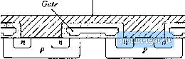 Drain 4.2.2 Metal Oxide Semiconductor Field-Effect Transistor (MOSFET) The power MOSFET is a modern power seraiconductt)r device having gate lengths close to t)ne micron. The power device is comprised of many small parallel-connected enhancement-mt)de MOSFET cells, which cover the surface of the silicon die, A cross-section of one cell is illtistrated in Fig. 4.26, Ctirrent flows vertically through the silicon wafer: the metallized drain connection is made on the bottom of the chip, while the metallized source connection and polysilicon gate are on the top surface. Under normal operating conditions, in which v,, > 0, bt)th the p-n and p-n junctions are reverse-biased. Figure 4.27(a) illustrates operation of the device in the off state. The applied drain-to-source voltage then appears across the depletion region of the junction. The fi~ region is lightly doped, such that the desired breakdown voltage rating is attained. Figure 4.27(b) illustrates operation in the on state, with a sufficiently large positive gate-to-source voltage. A channel then forms at the surface of the/? region, underneath the gate. The drain current flows through the n~ region, channel, и region, and out through the source contact. The on-resistance of the device is the sum of the resistances of the n region, the channel, the st)urce and drain contacts, etc. As the breakdown voltage is increased, the on-resistance becomes dominated by the resistance of the n~ region. Since there are no minority carriers to cause conductivity modulation, the on-resistance increases rapidly as the breakdown voltage is increased to several hundred volts and beyond. Yhep-fi junction is called the body diode:, as illustrated in Fig. 4.27(c), this junction forms an effective diode in parallel with the MOSFET channel. The body diode can bectme forward-biased when the drain-to-soiirce voltage v ,(t) is negative. This diode is capable of ct)nducting the full rated current of the MOSFET. However, most MOSFETs arc not optimized with respect to the speed of their body diodes, and the large peak currents that flow during the reverse rectjvery transition of the body diode can cause device failure. Several manufacturers produce MOSFETs that contain fast recovery bt)dy diodes; these devices are rated to withstand the peak currents during the body diode reverse recovety transition. Typical ([-channel MOSFET static switch characteristics are illustrated in Fig. 4.28. The drain current is plotted as a function of the gate-to-source voltage, for various values of drain-to-source voltage. When the gate-to-source voltage is less than the threshold voltage Vj the device operates in the off state. A typical value of V, is 3 V. When the gate-to-source voltage is greater than 6 or 7 V, the device operates in the on state; typically, the gate is driven to 12 or 15 V to ensure minimization of the forward voltage drop. In the on state, the drain-to-source voltage V is roughly proportional to the drain current |