
|
| |
|
Строительный блокнот Introduction to electronics (20.47) The switch conversion ratio \l is thus linQlted to a value slightly less than 1. The averaged waveforms of converters containing half-wave ZCS quasi-resonant switches can now be determined. The results of the analysis of PWM converters operating in the continuous conduction mode can be directly adapted to the related quasi-resonant converters, simply by replacing the duty cycle d with the switch conversion ratio pi. For the buck converter example, the conversion ratio is (20.48) This result could also be derived by use of the principle of inductor volt-second balance. The average voltage acToss the filter inductor is (fiV - V). Upon equating this voltage to zero, we obtain Eq. (20.48). In the buck converter, /j is equal to the load current I, while V, is equal to the converter input voltage V. Hence, thequantity./, is (20.49) Zero current switching occurs for 1<Л {2t).50) The output voltage can vary over the range (20.51) which nearly coincides with the PWM output voltage t;mge 0 < V< V. A htK)St converter employing a half-wave ZCS quasi-resonant switch is illustrated in Fig. 20.17. The conversion ratio of the boost converter is given by V 1-Ц (20.52) Fig. 2(1,17 Booat converter contairiing a half-w.ivc ZCS quasi-rcsoitant switch. L hit) L о r о 2 + ViWC V The half-wave switch ti)nversii)n ratio i is again given by Eqs. (20.44) to (20.46). For the boost coti-vetter, the applied .switch voltage V, is equal to the output voltage V, while the applied switch current is equal to the filter inductor current, orHence, the quantity uf, is , .lia ko (20.53) Also, the input current } of the boo.st converter is teiated to the load current / according to Equations (20.52) to (20.54), in coiijiiactioa with Eqs. (20.44) to (20.46), describe the averaged wave-fornts ofthe half-wave quasi-resotiant ZCS boost cotiverter. 20.2.3 The FuU-Wave ZCS Quasi-Resonant Switch Cell The full-wave ZCS quasi-resonant switch cell is illustrated in Fig. 20.8(d). It differs from the half-wave cell in that elements D and Gj are connected in antiparailel, to form a current-bidirectional two-quadrant switch. Typical tatik inductor current and tank capacitor vohage waveforms ate illustrated in Fig. 20.18. These waveforms are similar to those ofthe half-wave case, except that the Q]ID\ switch interrupts the tank inductor cutrent i,(t) at it.s second zero-crossing. While ilt) is negative, diode conducts, and transistor 0] can be turned off at zero current. The analy.sis is nearly the same as for the half-wave са.че, with the exceptioti of subinterval 2. The subinterval 2 angular length fi and final voltage V.j can be shown to be (yj (lialfwave) iTt + .sm 1 27t-sin-(yJ (full wave) (20.55) Subinierval: Fig, 20,18 Tank inductor cunent and capacitor voltage wavefcirmji, for the full-wave ZCS quasi-resonant switch cell of Fig, 20,8(d), Conducting Qi devices: p  Soft Swiicliifsg Fig. 20.19 Clittracteri.itics of the fuU-wave ZCS quasi-resonaiit switch. 0.S 0.6 - ZCS boundary 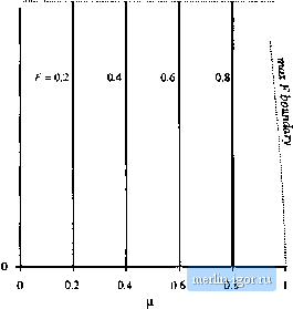 0.4 - 0.2 - 1 -J]) (half wave) 1 - (full wave) (20.S6) In eithei са.че, the switch conversion ratio /iis given by Eq. (20.42). Forthe full-wave switch, one obtain.? where Pf(J,) is given by i J, + 27Г - sin - V,) + 7 (1 -/Т) In the fnll-wave case, PiU,) is essentially independent of/: (20.58) (20.59) The worst-case deviation of/(У) from 1 occurs as tends to 1, where P(JJ tends to 0.%. So Pj(J,} lies within 4 of unity forO < /, < 1. Hence, for the full-wave case, it is a good approximation to express the switch conversion ratio as (20.50) The full-wave quasi-resonant switch therefore exhibits voltage-source output characteristics, controllable |