
|
| |
|
Строительный блокнот Introduction to electronics Softswitching JiCf) Subinterval: 1 9 = ш/ 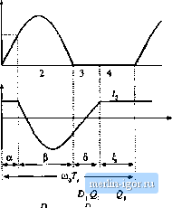 Conducting devices: X Fig, 20,24 A ZVS quasi-resonant buck converter: (a) circuit, (b) tank waveforms, of the PWM switch, the peak transistor blocking voltage is substantially increased. This leads to increased conduction loss, because transistor on-resistance increases rapidly with rated blocking voltage. 20.3.2 The Zero-Voltage-Switching Multiresonant Switch The resonant switch network of Fig. 20.25 contains tank capacitor in parallel with diode Dj, as in the ZCS switch network of Fig. 20.22. In addition, it contains tank capacitor in parallel with the SPST switch, as in the ZVS switch network of Fig. 20.23. In consequence, all semiconductor elements switch at zero voltage. This three-element resonant switch network is known as the zero-voltage-switching multiresonant switch (ZVS MRS). Since no seiniconductor output capacitances or diode recovered charges lead to ringing or switching loss, the ZVS MRS exhibits very low switching loss. For the same reason, generation of electromagnetic interference is reduced. A half-wave ZVS MRS realization of the buck converter is illustrated in Fig. 2().2й. In a typical design that must operate over a 5:1 load range and with 0.4 < )i <0,6, the designer might choose a maximum f of 1.0, a maximum 7of 1.4, and C;/C, = 3, where these quantities are defined as follows: ТЛЛГ Fig. 20,25 Elimination of eonverter low-frequency elettienU гейиееь the ZVS rnultireaonanl switch cell to this network. (20.65) As tistial, the conversion ratio i.s tlefined as - Vj/V,. The resulting peak transistor voltage ft)r this typical design is approximately 2.8Vj, while the peak transistor current is 2/. Hence, conduction losses are higher than in an equivalent PWM switch. The range of switch conversion ratios ji is a function ofthe capacitor ratio CJC/, in a good design, values of fi ranging from nearly one to nearly zero can be obtained, with a wide range of dc load currents and while maintaining zero voltage switching. Analysis and design charts for the ZVS MRS are given in [5-8]. Results for the typical choice Cj = 3C\ are plotted in Fig. 20.27. These plots illustrate how the switch conversion ratio (l varies as a function ofload current and switching frequency. Figure 2().27(a) also illustrates the boundary of zero-voltage switching: ZVS is lost for operation outside the dashed lines. Decreasing the ratio of Q to Cj reduces the area ofthe ZVS region. Other resonant converters in which ail semiconductor devices operate with zero voltage switching are known. Examples include some operating mtKles of the parallel and LCC resonant converters described in Chapter 19, as well as the ciass-E converters descriljed in [10-12]. (,(0 2(0. ТППР R < V Fig, 20.26 Half-wave ZVS multiresonant buek converter, 78Й Scf! Switching 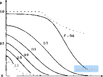 OJ IJO 1.3 2.0 2.5 J 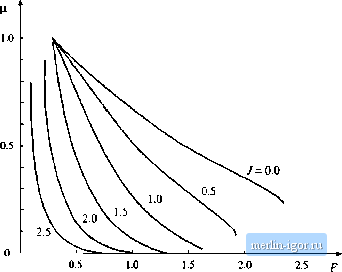 Fifi. 20.27 Cotivwsion ratio fi lot tlic multi-resoiiuoi .switch with C= ЗС,.: (a) coiivcraoii ratio д vs. nomialized current J {solid lines: conversion ratio; dashed lines: boundaries of zero-vultage switching), (b) conversion ratio ;r vs, noinialized switching frequency |