
|
| |
|
Строительный блокнот Introduction to electronics 20.3.3 Quasi-Square-Wave Resonant Switches 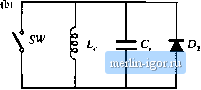 Another basie dass of resonant switch networks is the (a) quasi-square wave converters. Both zero-voltage switching and zero-current switching versions are known; the resonant tank networks are illustrated in Fig. 20.2E. In the network of Fig. 20.28(a), all semiconductor devices are effectively in series with the tank inductor, and hence operate with zero-current switching. In the network of Fig. 2().28(b), ail semiconductor devices iire effectively in parallel with the tank capacitor, and hence operate with zero-voltage switching. Figure 20.29 illustrates implementation of a zero current switching quasi-square wave resonant switch, in a buck ct)nverter with input filter. Elements t-and C-are large in value, and constitute a single-section L-C input filter. Elements iand tform the .series resonant tank: these elements are placed in series with input fiiter capacitor Cj. Since and Cj are connected in series, they can be combined into a single small-value capacitor. In this zero-current-switching converter, the peak transistor current is identical to the peak transistor current of an equivalent PWM converter. However, the peak transistt)r blocking voltage is increased. The ZCS QSW resonant switch exhibits a switch conversion ratio ji that is restricted to the range 0 < fl <Q.5. Analysis of this resonant switch is given in [13-14]. A buck converter, containing a zero-voitage-switching quasi-square wave (ZVS QSW) resonant switch, is illustrated in Fig. 20.30. Typical waveforms are given in Fig. 20.31. Since the tank inductor and the output filter inductor L iire connected in parallel, these two elements can be combined into ii single indtictt)r having a small value nearly equal to L. Analyses of the ZVS QSW resonant switch are given in [14,15,18]. A related full-bridge converter is described in [16]. The ZVS QSW resonant switch is notable because zero voltage switching is obtained in all semiconductor devices, yet the peak transistor voltage is identical to that of an equivalent PWM switch [13]. However, the peak transistor currents are increased. Characteristics of the zero-voltage-switching quasi-square wave resonant switch are plotted in Fig. 20.32. The switch conversion ratio (l - Vj/V, is plotted as a function of nt)rmalized switching fre- Fig. 2(1.28 Elimination of converter low-frequency elements reduces the quasi-squaie-wave switch cells to these networks; (a) ZCS quasi-square-wave network, (h) ZV.S quasi-square-wave network. 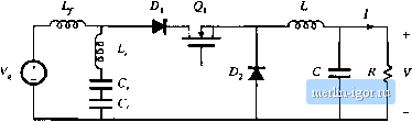 Fig. 20.2У Incorporation of a ZCS quiisi-sqLiare-wave resonant switch into a buck converter containing an L-C input filter. 788 Soft Swilching 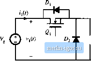 hit) ТЛПР Fig. 20.30 incorporation ofa ZVS quasi-square-wave resonant swiich into a butk converter. Fig, 20,31 Waveforms of the ZVS qitasi-square-wave resonant swilcli converter nf Fig, 2U.3ti. 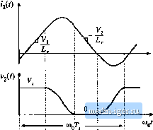 Conducting devicts: D Ol i O, I X \ Fig, 20.32 Characteristics of the ZVS quasi-square wave resonant switch network; switch conversiun ratio , as a fnnotlon of F and J, Dashed line: ZVS boundary. 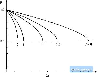 1.0 F © v,(0 Fig, 20.33 Quaai-square wave ZVS buck cotiverter containing a synchronous rectifier. quency Fund nonnaiized output currenti. where these quantities are defined as foiiows: (20.66) In addition, the zero-voltage-switching boundary is piotted. It can be seen that the requirement for zero-voltage switching limits the switch conversion ratio Ц to the range 0.5 < ;t < I. In consequence, the buck converter of Fig. 20.30 cannot produce output voltage.s less than O.SV without losing the ZVS property. A version which attains 0 Й ;i < 1, at the expense of increased transistor voltage stress, is described in [17]. In addition, the two-switch version of the ZVS-QSW switch can operate with ZVS for fl < 0.5. A useful variant of the converter of Fig. 20.30 involves replacement of the diode with a synchronous rectitlei, as illustrated in Fig. 20.33 [8,9]. The second transistor introduces an additioital degree of freedom in control ofthe converler, because this transistor can be allowed to conduct longer than the diode would otherwise conduct. This fact can be used to extend the region of zero-voitage switching to conversion ratios approaching zero, and also to operate the converter with constant switching frequency. Typical tank element waveforms for the ciicuit of Fig. 20.33 i\re illustrated in Fig. 20.34. These waveforms resemble diose of the single switch case, Fig. 20.31, except that the tank cturent is negative while transistor conducts. The duty cycle D is defined with respect to the turn-off transitions Fig. 20J4 Waveforms for the two-switch QSW-ZVS converter OfFig, 20.33. 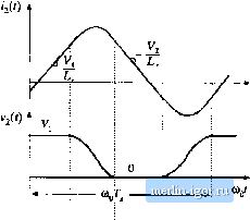 Conducting [ devices: q,] x |