
|
| |
Строительный блокнот Introduction to electronics
Fig. 2035 Conveivsiori ratio ju, а.ч a fuiictioti of duty cycle D and nurmalized load tiirrent J, fur the twu-switcli QSW-ZV.S switch illustrated in Fig. 20.33. Curves are plotted fur coitstant-frequency coittrol wiih F - O.S. The dashed line is the /ern-voliage switching Iwundary, of transistors Qj and Q, as illustrated. Characteristics of the two-switch QSW-ZVS switch network ;ue plotted in Fig. 20.35, for the case of constant switching frequency at F = 0.5. The boundary of zero-voltage switching is also illustrated. Operation at a lower value of F causes the ZVS boundary to be extended to larger values of/, and to values of p. that more closely approach the extreme values = 0 and /J = 1. To the commutation intervals can be neglected, one would expect that the switch conversion ratio /lis simply equal to the duty cycle D. It can be seen from Fig. 20.35 that this is indeed the case. The characteristics are approximately horizontal lines, nearly independent of load current 7. Zero-voltage .switching quasi-.square wave converters exhibit very low switching loss, because all semiconductor elements operate with zero-voltage switching. In the constant-frequency case containing a synchronous rectifier, the converter behavior is nearly the same as for the hard-switched PWM case, since \L~D. The major disadvantage is the increased conduction toss, caused by the reversal of the inductor current. 20.4 SOFT SWITCHIN(; IN PWM CONVERTERS The quasi-square wave approach of the previous section is notable because it attains zero-voltage switching without increasing the peak voltage applied to the transistor. Several related soft-switching approaches have now become popular, which also attain zero-voltage switching without increasing the transistor peak voltage stress. In this section, popular zero-voltage switching versions oftite full bridge, forward, and flyback converters, as well as the voltage-source inverter, are briefly discussed. 20.4Л The Zero-Voltage Transition Full-Bridge Converter It is possible to obtaiti soft switching in other types of converters as well. An exatiipie is the zero-voitage transition (ZVT) convetter based on the full-bridge transformer-isolated buck converter, illustrated in Fig. 20.36 [25-28]. The transistor and diode output capticitiittces ate represented iu the figure by capacitances Cj,. Commutating indnctor L. is placed in series with the transformer; the net inductance L. includes both transformer leakage inductance and the inductance of an additional discrete element. This inductor causes the full-bridge switch tietwork to drive an effective itiductive load, and results in zero-vohage switching ofthe primary-side semiconductor devices. Although the waveforms are not sinusoidal, it can nonetheless be said that the switch tietwork output curretit Цс) lags the voltage v(/), because the zero crossings of uccur after tlie ZVS switching ttan.sitiDns Lire totnpieted. The output voltage is controlled via phase control. As illustrated in Fig. 20.37, both halves of the bridge switch network operate with a 50% duty cycle, and the phase difference between the half-bridge switch networks is controlled. The idealized waveforms of Fig. 20.37 neglect the switching transitions, and the subintervai numbers correspond to those of the more detailed Fig. 20.38. The phase shift variable ф lies in the range 0£ф < 1, and assumes the role ofthe duty cycle d in this converter. The qnan-tity Ф is defined as (20.67) By volt-second baiance on the secondary-side filter inductor, the conversion ratio М{ф) is expressed as (20.ЬЯ) This expression neglects the lengths ofthe switching transitions. .Although the circuit appears symmetrical, the phase-shift control scheme introduces an asymmetry that causes the two haif-bridge switch networks to behave tjuite differently during the switching transitions. During subintervals 4 and 10, energy is actively transmitted from the source through the switches and transformer. These subintervals are initiated by the switching of the half-bridge network 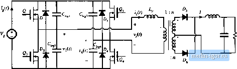 Fig. 20.36 Zero-voltage transition convener, based on the full-bridge isolated buck converter. V4(0 а-Ф)г,/2- Subinterval: Conducting Qi devices: д - v Kig. 20,37 Iliase-shifl tontiol of the ZVT fulJ-bridge converler. Switching transitlotis arc neglected in this figure, and subinterval numbering follows Fig. 20.38, composed of the elements Q B Q2, and ZJ, called the passive-to-activc (P~A) transition [27]. Sub-intervals 4 and 10 are tertninated by the switching of the half-bridge networlt cotnprised by the eletnents Q31 Dj, Q, and D, called the active-to-passive (A-P) transition. The turn-on and turn-off switching processes of this converter are similar to the zero-voltage-switching turn-off process described in the previous section. Detailed primary-side waveforms are illustrated in Fig. 20.38. During subinterval 0, it conduct. !f the transformer magnetizing current Ij is negligible, then the commutating inductorcurrent is given by ijtg) = -nI, where 7 is the load current. The passive-to-active transition is initiated when transistor is tttrned off. The negative i. then causes capacitors C, and C to charge, increasing V2(r). Dttring subinterval 1, , L, Cfr and С,,2 form a resonant network that rings with approximately sinusoidal waveforms. If sufficient energy was initially stored in Z ., then vW eventually reaches V terminating subinterval 1. Diode />, then clamps vf/) to during subinterval 2. Transistor 2, is ttirned on at zero voltage during subinterval 2; in practice, this is implemented by insertion of a small delay between the switching transitions of transistors q2 and Qj. If Lj, does not initially store sufficient energy to charge the total capacitance (C + C,) irota V2 = 0 to = during subinterval 1 ,then 1*2(0 will never reach V. Switching loss will then occur when transistor 0 is turned on. This situation typically occurs at light load, where / is small. Sometimes, the design engineer may choose to simply accept this power loss; after all, other losses such as conduction loss are small at light load. An alternative is to modify the circuit to increase the energy stored in L. at |
|||||||||||||||||||||||