
|
| |
Строительный блокнот Introduction to electronics 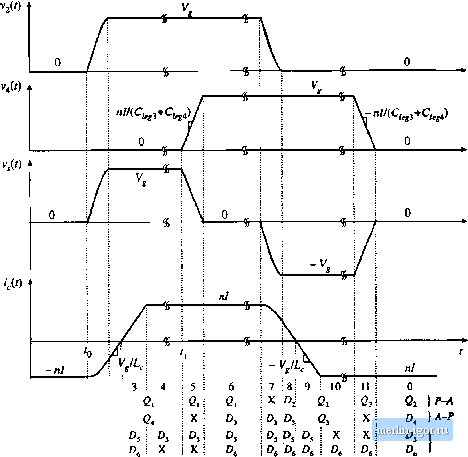 Subintervat: Conducting devices: Secondary diodes Fig. 20,38 Detailed diagram of [K-imary-side waveforms of the ZVT full-bridge converter, illustrating die zero-voltage switching mechanisms. Ait ideal transformer is assumed. r = Iq under light load conditions. One way to atcompli.sh this is to increase the transfortner magnetizing current ifjyiff) to a significant level; at the beginning of subinterval 1, 1. is then equal to fj.({()) = -n.l+ (;f{(())with ijy(fo) < 0. At light load where /is stnall, the magnetizing current maintains the required level of i. During subintervals 0, 1,2, and 3, secondary-side diodes and both conduct; hence, zero voltage appears across all transformer windings. In consequence, voltage is applied to comtnutating inductor during subintervals 2 and 3, causing i{i) to increase with slope V/L. Current ijj) reaches zero at the end of subinterval 2, and increases to the positive value + n/ at the end of subinterval 3. The reversal of polarity of ijf) enables zero-voltage switching during the next switching transitions, subinterval 5 and subintervals 7~У. At the end of subinterval 3, the current in ditxle has decreased to zero. then becotnes reverse-biased, with zero-cnrrent switching. At this instant, ditxle must begin to block voltage 2nV,. 794 Sofi Switching The output capacitance of D; prevents the voltage from changing immediately \o2nV; instead, the resonant circuit formed by and the output capacitance begins to ring in a manner similar to Fig. 4.54. Peak voltages are typically observed that are considerahiy in excess ofTnV, and it is usually necessary to add voltage-clamp snubbers that prevent the secondary-side diode voltages from exceeding a safe value. Several dissipative and non-dissipative approaches are discussed in [26-2S]. The active-to-passive switching transition occurs during subinterval 5, This subinterval is initiated when transistor is turned off. The positive current (.(f) is equal to the reflected load current nl, and charges capacitors Cf- and C fromi4 = t* to = V. Subinterval 5 ends when v. reachesV,; Diode then becomes forward-biased. Transistor is then turned on during subinterval 6, with zero-voltage switching. This is typically implemented by insertion ofa small delay between the switching of transistors and Because is constant and equal to during subinterval 5, the active-to-passive transition maintains zero-voltage switching at all load currents. Circuit behavior during the next half switching period, comprising subintervals 6 to 11, is symmetrical and therefore similar to the behavior observ-ed dtiring subintervals 0 to 5. The switching transitions of transistors Q, and are passive-to-active transitions, and occtir with zero-voltage switching provided that sufficient energy is stored in as described above. The switching transitions ofQj and 64 are active-to-passive, and occur with zero-voltage switching at all loads. The zero-voltage transition converter exhibits low primary-side switching loss and generated EMI. Conduction loss is increased with respect to an ideal PWM full-bridge topology, because of the current Jj, that circulates through the primary-side semiconductors during subintervals 0 and 6. However, this increase in conduction loss can be small if the range of input voltage variations is narrow. This soft-swhching approach has now found commercial success, 20.4.2 The Auxiliary Switch Approach A similar approach can be used in forward, flyback, and other transforraer-isolated converters. As illustrated in Fig. 20.39, an active-clarap sntibber network consisting of a capacitor and auxriiary MOSFET Q2 is added, that is effectively in parallel with the original power transistor Q[ [29]. The MOSFET body diodes and output drain-to-source capacitances, as well as the transformer leakage inductance Lf, participate in the circuit operation. These elements lead to zero-voltage switching, with waveforms similar to those of the ZVT full-bridge converter of Section 20.4.1 or the two-transistor QSW-ZVS switch of Section 20.3.3. The transistors are driven by complementary signals; for example, after turning off Q the controller waits for a short delay tirae and then ttirns on Й. The active-clamp snubber can be viewed as a voltage-clamp snubber, similar to the dissipative snubber illustrated in Fig. 20.6. However, the snubber contains no resistor; instead, MOSFET allows bidirectional power flow, so that the energy stored in capacitor C, can flow hack into the converter The voltage v, can be fotind by volt-second inductance on the transformer magnetizing inductance. If the lengths of the commutation intervals are neglected, and if the voltage ripple in 1,(0 can be neglected, then one finds that The voltage is effectively an unloaded output of the converter. With the Iwo-quadrant switch provided by Q2, this output operates in continuous condtiction mode with no load, and hence the peak voltage of Qi is clamped to the minimum level necessary to balance the volt-seconds applied to the transformer magnetizing inductance. 20.4 Soft Switch ing in P WM Con verrers 795
4!]
0. I 7 Fig. 20.39 Attive-clamp snubber circuits; (ti) foi wai d convenor, (b> flyback converter.  Fig. 20.40 Waveforms of the iictive-cbmp snubber circuit of Fig. 20.39(a). |