
|
| |
|
Строительный блокнот Introduction to electronics Softswitching Typical waveforms for a forward converter incorporating an active-clamp snubber are illustrated in Fig. 20.40. The current i((l) reverses direction while conducts. When £?j turns off, capacitor Сд, begins to discharge. When Vj reaches zero, the body diode of Q, becomes forward-biased. Q, can then be turned on at zero voltage. An added benefit of the active clarap snubber, when used in a forward converter, is that it resets the transformer. Consequently, the converter can operate at any duty cycle, including duty cycles greater than 50%. When the converter raust operate with a wide range of input voltages, this can allow substantial improvements in transistor stresses and efficiency. The MOSFETs in Fig. 20.39 operate with zero-voltage switching, while the secondary-side diodes operate with zero-current switching, This approach is quite versatile, and similar auxiliary circuits can he added to other converter circuits to ohtain zero-voltage switching [30,31]. 20.4J Auxiliary Resonant Cununutted Pole The auxiliary resonant commutated pole (ARCP) is a related circuit that uses an atixiliary four-quadrant switch (or two equivalent two-quadrant switches) to obtain soft switching in the transistors ofa bridge inverter circuit [32-34]. This approach finds application in dc-ac inverter circuits. Figure 20.41 illustrates a half-bridge circuit, or one phase of a three-phase voltage-source inverter, driving an ac load. This circuit can lead to zero-voltage switching that mitigates the switching loss induced hy the reverse recovery of diodes and D. Filter inductor /j is relatively large, so that the outptit current ij,t) is essentially constant during the resonant commutation interval. Capacitors Cj, are relatively small, and model the output capacitances of the semiconductor devices. Inductor is also relatively small, and elements and C, form a resonant circuit that rings during part of the commutation process. Semiconductor switching devices Q, Q, Dj, and form an auxiliary four-quadrant switch that turns on to initiate the resonant commutatiDii process. Typical corarautation waveforms are illustrated in Fig, 20,42(a), for the case in which the ac load current i is positive. Diode is initially conducting the output current i . It is desired to turn off Dj and turn on Oj. with zero-voltage switching. This is accomplished with the following sequence: interval I. Turn on uansisLor (j. Devices £>2i Й3, and D4 conduct. Interval 2. When the current in reaches zero, Dj turns off. A resonant ringing interval occurs. Interval 3. When the vohiige v reaches V/2, diode D, begins to become fotwJrd-biased. Transistor Q is then immediately turned un at zero voltage. M I M p ТЛЛР (!) T T Fig, 20.41 Half-bridge ciicuit driving an ae load, with ARCP zcro-voltugc switching. Load
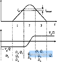 Ffg. 10.42 Waveforms of the ARCP circuii of Pig. 20.41: (a) basic ivavefornisi, <b) with current boost. At the cotnjiusion of interval 3, teaches zero and diode £>j turns off. For negative current, the process for commutation of diode D is similar, except that transistor and diode O-j conduct the resonant current (ДО- One issue related to the wavefonns ofFig. 20.42(a) is that the circuit always operates at the boundary of zero-voitage switching. At the end of interval 2, diode D, i.s not actually forward-biased, because its current never actually becomes positive. Instead, transistor Q] should be turned on at the beginning of interval 3. If transistor is gated on late, then the continued ringing will cause voltage Vg,i(t) to decrease, and zero-voitage switching will be lost. To further assist iti the zero-voitage switching commutation process, transistor C?2 *-an be turned on while conducts, as illustrated in Fig. 20.42(b). Transistor Q2 is used to lengthen the duration of interval 1: now, when the current гДО exceeds current i by an amount then the controller turns off Q2 to end interval 1. This causes diode ZJ, to become forward-biased during the beginning of interval 3. Transistor is then turned on with zero-voitage switching, while is conducting. Regardless of whether the circuit operates with the waveforms of Fig. 20.42(a) or (b), the ARCP approach eliminates the switching loss caused by the reverse recovery of diodes and Dj. Unlike the previous circuits of this chapter, the ARCP has no circulating currents that cause conduction loss, because the tank inductor current ijil) is nonzero only in the vicinity of the commutation interval. The approach ofFig. 20.42(a) does not completely eliminate the loss caused by the device output capacitances. This loss is eliminated using the current boost of Fig. 20.42(b), but additional conduction loss is incurred because of the increased pealt iXO- The waveforms of Fig. 2().42(b) may, in fact, lead to reduced efficiency relative to Fig. 20.42(a)l 20.5 SUIWIWARV OF KEY P(HNTS In a resonant switch converter, the switch network of li PWM converter is replaced by a switch neiwork containing resonant elements. The resulting hybrid convener combines the properlies uf the resonant switch network and the pureni PWM convener. Analysis of a resonant or soil-switching switch cell involves determination oflhe switch conversion ratio /1. The resonani switch wiivelorms are determined, unJ are then averaged. The switch conversion ralio Ц is 798 Softswitching л generalization of the PWM CCM duly cycle d. The results of ihe averaged analysis of PWM converters operating in CCM can be directly adapted to the related resonant switch converter, simply by replacing d with p.. In the zero-currenl-switching quasi-resonant switch, diode operates with zero-voltage switching, white transistor Q and diode D[ operate with zero-current switching. In the zero-voltage-switchingquasi-reso-nant switch, the transistor and diode D, operate wilh zero-vidtage switching, while diode Dj operates with zero-current switching. In the zero-voltjge-swilching inultiresonant switch, all seiniconduclor devices operute with zero-voitage switching. In consequence, very low switching loss is observed. In the quasi-sqnare-wave гего-vohage-switching resonani switches, aii semiconductor devices operate with zero-voltage switching, and with peak voltages equal to those of the parent PWM converter. The switch conversion ratio is restricted to the range 0.5 <р< i. Versions containing synchronous rectifiers can operate with values of/г approaching zero. Tbe zero-vollage transition approach, as well as the active-clamp snubber approach, lead to zero-voltage switching of the transistors and zero-current switching of the diodes. These approaches have been successful in substantially improving the efficiencies of transformer-isolated converters, The auAiliary resonant Commutated pole induces zero-voltage switching in bridge circuits such as the voltae-sOLirce inverter. References [1] P. Vira,\RELLi, Forward Converter Switching al Zero Current, U.S. Patent 4,415,959, Nov. 1983. [2] K. Liu, R. Oruganti, and F. C. Lee, Resonant Switches: Topologies and Characteristics, IEEE Power Electronics Specialists Conference, 1985 Record, pp. 106-116. [3] M. F. ScHLECHT and L. F. Casey, Comparison of the Square-Wave and Quasi-Resonant Topologies, IEEE Applied Power Electronics Conference, 1987 Record, pp. 124-134. [4] K. Liu and F, C, Lee, Zero Voltage Swilching Technique in Dc-Dc Converters, IEEE Power Electronics Specialists Conference, 1986 Retold, pp. 58-70. [5] W, A. Tabisz and F. C. Lee, Zero-Voltage-Switching Multi-Resonant Technique-A Novel Approach to Improve Performance of High-Frequency Quasi-Resonant Converlers, IEEE Power Electronics Speciali.its Conference. 19SS Record, pp. 9-17. [6] W. A. Tabisz, M. M. Iovanovic, and F. C. Lee, High Frequency Multi-Resonant Converter Technology and Its Appiicutions, lEE International Conferetice on Power Electronics atid Variable Speed Driies. July 17-19, 1990. p. 1-8. [7] R. Farrington, M. Jovanovic, and F. C. Lee, Constant-Frequency Zero-Voltage-Switehed Multi-Res- onant Converlers: Analysis, Design, and Experimental Rsnuili, IEEE Power Electronics Specialists Conference, 1990 Record, pp. 197-205. [8] D. M.KSIMOVlt:, Synthesis of PWM and Quasi-Resonunl Dc-lo-Dc Power Converlers, Ph.D. thesis, California InstilLLle of Technology, January 1989. [9] X. Zuou, X. ZiUKO, J. Ltu, P. Wono, J. Chen, H. Wu, L. Amoroso, F. Lee, and D. Chen, Invesuga- tion of Candidate VRM Topologies for Future Microprocessors, IEEE Applied Power Electronics Conference, 1998 Record, pp. 145-150. |
|||||||||||||||||||||||||||||||||||||||||||||