
|
| |
|
Строительный блокнот Introduction to electronics 7ZZ ZD Source 7ZZZZZZZZ --J
Depletion rtgion Fig. 4.27 Operation of the [sowei-MOSFFT: <a) in tlie off state, f, appears across the depletion region in tlie n~ region; (Ъ) curreiil flinv thnjngli the conducting channel in the on state; (c) body diode due to the f)-M junction. 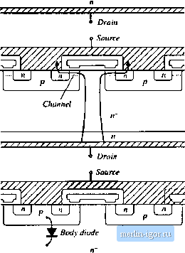 Draifi /д. The MOSFET is able to conduct peak currents well in excess of its average current rating, and tlie nature of tlie static characteristics is unclianged at high current levels. Logic-level power MOSFETs are also available, which operate in the on state with a gate-to-source voltage t)f 5 V. A few/-channel devices can be obtained, but their properties are inferior to those of equivalent n-channel devices. The on-iesistauce and forward voltage drop of the MOSFET have a positive temperature coefficient. This property makes it relatively easy to parallel devices. High current MOSFET modules are available, containing several parallel-connect chips. The major capacitances of the MOSFET are illustrated in Fig. 4.29. This model is sufficient for ША - Fig. 4.28 Typical static charatiCTistits of a power MOSFET, Dniin current i is plotted vs. gate-to-.чоигсе voltiige Vg-, for various values of draiii-to-source voltage  qualitative understantiing of the MOSFET switching behavior; more accurate models account for the parasitic junction field-effect transistor inherent in the DMOS geometry. Switching times of the MOSFET are determined essentially by the times required for the gate driver to charge these capacitances. Since the drain current is a function of the gate-to-soiirce voltage, the rate at which the drain current changes is dependent on the rate at w hich the gate-to-soitrce capacitance is charged by the gate drive circuit. Likewise, the rate at which the drain voltage changes is a function of the rate at which the gate-to-drain capacitance is charged. The drain-to-source capacitance leads directly to switching loss in PWM conveitet.4, since the energy .stored in this capacitance is lost during the transi.stor turn-on transition. Switchitig loss is discussed in Section 4.3. The gate-to-source capacitance is essentially linear. However, the drain-to-soitrce and gate-to-drain capacitances are strongly nonlinear: these incremental capacitances vary as the inverse square root of the applied capacitor voltage. For example, the dependence of the incremental drain-to-source capacitance can be written in the form (4.4) where and Vg are constants that depend on the constritction of the device. These capacitances can easily vary by several orders of magnitude as f. varies over its nortnal operating range. For v. Vf Eq. Fig. 4.2il MOSFET equivalent circuit which accounts for the liody diode and effective termitial capacitances. Table 4.2 Charuderi.stics of several commercial /i-cliattncl power MOSFETa
These expressions are used in Section 4.3.3 to determine the switching loss due to energy stored in C, Characteristics of several commercially available power MOSFETs are listed in Table 4.2. The gate charge is the charge that the gate drive circuit must supply to the MOSFET to raise the gate voltage from zero to .some .specified value (typically 10 V). with a specified value of off state drain-to-source voltage (typically 80% of the rated Vj. The total gate charge is the sum of the charges on the gate-to-drain and the gate-to-source capacitance. The total gate charge is to some extent a measure of the size and switching speed of the MOSFET. Unlike other power devices, MOSFETs are usually not selected on the basis of their rated average current. Rather, on-resistance and its influence on conduction loss are the limiting factors, and MOS-FET.s typically operate at average currents somewhat less than the rated value. MOSFETs are usually the device of choice at voltages less than or equal to approximately 400 to 500 V. At these voltages, the forward voltage drop is competitive or superior to the forward voltage drops of minority-carrier devices, and the switching speed is significantly faster. Typical switching times are in the range 50 ns to 200 ns. At voltages greater than 4(K) to 5(X) V, minority-carrier devices having lower forward voltage drops, such as the IGBT, tire usually preferred. The only exception is in applications where the high switching speed overrides the increased cost of silicon required to obtain acceptably low conduction loss. 4.2.3 Bipolar Junction Transistor (BJT) A cross-section of an NPN power BJT is illustrated in Fig. 4.30. As with other power devices, currentflows vertically through the silicon wafer. A lightly doped n~ region is inserted in the collector, to obtain the desired voltage breakdown rating.The transistor operates in the off state (cutoff) when the?-n base-emitter junction and the p-ft base-collector junction are reverse-biased; the applied collector-to-emitter voltage then appears essentially across the depletion region of the р-я junction. The transistor operates in the on state (saturation) when bothjunctions are forward-biased; substantial minority charge is then present in the p and n~ regions. This minority charge causes the ;Г region to exhibit a low on- |