
|
| |
|
Строительный блокнот Introduction to electronics on seleuled parts of the system, and over short lime intervals involving a few switching cycles al most. Devices for power converters, and detailed physical device modeling, are areas of active research and development beyond the scope of this book. 2. Simplified device models. Since an on/off switching transition usually takes a small fraction of a swilching cycle, the basic operation of swilching power converlers can be explained using simplified, idealized device models. For example, a MOSFET can be modeled as a swiich with a small (ideally zero) on-resistance ff, when on, and a very large off-resistance (ideally an open circuit) when off. Such simplified models yield physical insight into the basic operation of switching power converters, and provide the starting point for developments of analytical models described throughout this book. Simplified device models are also useful for time-domain simulations aimed at verifying converler and controlleroperation, switching ripples, currenl and vollage stresses, and responses lo load or input transients. Since device models are simple, and details of switching transitions are ignored, tasks lhat require simulations over many switching cycles can be completed efficiently using gen era!-purpose circuii simulators. In addition, specialized tools have been developed lo support fast transient simulation ofswilching powerconverters based on idealized, piecewise-iinear device models [1-7], or a combination of piecewise-iinear and n(jnlinear models [8]. 3. Averaged converter models. Averaged models that are well suited for prediction of converter sleady-state and dynamic responses are discussed throughout this book. These models are essential design tools because they provide physical insight and lead lo analytical results that can be used in the design process to select component parameter values foragiven set of specifications. In the design verification step, simulations of averaged converter models can be performed to test for losses and efficiency, steady-stale voltages and currents, stability, and large-signal transient responses. Since switching transitions and ripples are removed by averaging, simulations over long lime intervals and over many sets of parameter values can be completed efficiently. As a result, averaged models are also well suited for simulations of large electronic systems lhat include swilching converlers. Furthermore, since large-signal averaged models are nonlinear, but lime-invariant, small-signal ac simulations can be used tu generate various frequency responses of interest. Selected references on averaged converl:er modeling for simulation are listed at the end of this chapter [9-18]. Averaged models for computer simulation are covered in diis appendix. Based on the material presented in Seclion 7.4, averaged switch models for computer simulation of converters operating in continnous eonduction mode are described in Section B.l. Application examples include finding SEPIC dc conversion ratio and efficiency, tind huge-signal transient responses nf a buck-boost converter. Section B.2 describes an averaged switch model .suitable for simulation nf converters that may operate cither in continuous conduction mode or in di.scontinuous conduction mode. Application examples include finding SEPIC open-loop frequency responses in CCM and DCM, loop-gain, phase margin and closed-loop responses of a buek voltage regulator, and current harmonics in a DCM boost rectifier. Ba.scd on the results from Chapter 12, a simulation model for converters with current programmed control is described in Section B.3, together with a buck converter example that coinpnies control-to-output frequency responses with current programmed control against duty-cycle control. It is assujned that the reader is familiar with basics of Spice circuit sitnulations. All sitnulation models and examples in this appendix tuc prepared u.sing the PSpicc circuit simulator [19]. Netlists are included tn help explain details of model implementation and simulation analy.sis options. U.sually, instead of writing nedi.sts, the user would enter circuit diagrams and nnalysis options from a front-end schematic capture tool. The examples and the library switch.lib of subcircuit models described in this appendix are available on-hne. Similar models and examples ean be constructed for use with other simulation tools. Jl(f) 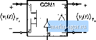 * Subcircuil: ССЫ1 Applicalion: two-switch PWM converters * Limitations: ideal switches, CCM qnly, no transformer * Raranneters: none Modes; * 1: transistcr positive (drain for an n-channet MOS) * £: transistor negative (sourt for an n-channel MOS) * 3: diode cathode * i: diode anode * 5: duty cycle cootrul input .subcktCCMt 12 3 4 5 Ell 2value=((1-v(5))*v(3,4)/v(5)} Gd 4 3 value={(1-v(5))i(Et)Af<5)) .ends Fig. B.l Averaged switch model CCM I; (a) the general two-switeh network: (b) symbol for the averaged .switch svibcitcuit model; (c) PSpice netlist of the sLibcir-cuit. AVERAGED SWITCH IVIODELS FOR CONTINUOUS CONDUCTION IVIODE The central idea of the averaged switch modeling described in Secnon 7.4 is to identify a switch network in the converter, and then to find an averaged circuit model. The resulting averaged switch model can then be inserted into the convertercircuit to obtain a complete model ofthe ctjnverter. An important feature ofthe averaged switch modeling approach is that the same inodel can be used in many different converter configurations; it is not necessary to rederive an averaged equivalent circuit for each particular converter. This feature is also very convenient for construction of averaged circuit models for simulation. A general-puфose subcircuit represents a large-signal nonlinear averaged switch model. The converter averaged circuit for simulation is then obtained by replacing the switch network with this subcircuit. Based on the discussion in Section 7.4, subcircuits that represent CCM averaged switch models are described in this section, together with application examples. B.1.1 Basic CCM Averaged Switch Model The large-signal averaged switch intHlel for the general two-Switch network of Fig. 7.39(a) is shown in Fig. 7.39(c). A PSpice subcircuit implementation of this nitHlel is shown in Fig. B.l. The subcircuit has five nodes. The transistor port of the averaged switch network is connected between the nodes 1 and 2, while the diode port is comprised of nodes 3 and 4. The duty ratio d = v(5) is the control input to the sub-circuit at the node 5. The quantity v(5) is a voltage that is equal to the duty cycle, and that lies in the range zero to one volt. Figure B.l(c) shows the netlist of the subcircuit. The netlist consists of only ftnir lines of code and several coininent lines (the lines starting with *). The .subckt line defines the name (CCMI) ofthe subcircuit and the interface nodes. The value of the controlled voltage source which models, lhe Iransistor port of the averaged switch network, is written aeeording lo Eq. (7.136): Note lhat v(3,4) in lhe stibeircnit of Fig. B.l is equal lo the swiich network independent input (v2(f))j. Also, d(l) = v(5), and tf{t) - I - d(t) - 1 - v(5). The value of the controlled ctirrent sotirce G,, which models the diode port, is computed according to Eq. (7.137): The switch network independent input {i{t))j equals the current i(£,) through the controlled voltage source C,. The ends line completes the subcircuit netlist. The subcircuit CCMl is included in the model library switch.lib. An advantage of the subcircuit CCMl of Fig. B. 1 is that it can be used to construct an averaged circuit model for simulation of any two-switch PWM converter operating in continuous conduction mode, subject to the assumptions that the switches can be considered ideal, and that the converter does not include a step-up or step-down transforiner. The stibcirctiit can be further refined to remove these limitations. In converters with an isolation transformer, the right-hand side of Eqs. (B.l) and (B,2) should be divided by the transformer ttirns ratio. Inclusion of switch conduction losses is discussed in the next section. A disadvantage of the model in Fig. B.l is that Eqs. (B.I) and (B.2) have a discontinuity at duty cycle equal to zero. In applications of the subcircuit, it is necessary to restrict the duty-cycle to the range Following the approach oi this section, subcircuits can be constructed tor the large-signal averaged models of the buck switch network (see Fig. 7.50(a), and Eqs. (7.150)), and the boost switch network (see Fig. 7.46(a) and Eqs. (7.146)). An advantage of these models is that their defining equations do not have the discontinuity problem at = 0. B.1.2 CCM Averaged Switch Model that Includes Switch Conductitin Losses Let us modify the model of Fig. B.l to include switch conduction losses. Figure B.2 shows simple device models that include transistor and diode conduction losses in the general two-switch network of Fig. B.l(a). The transistor is modeled as an ideal switch in series with an on-resistance The diode is modeled as an ideal diode in series with a forAard vtdtage drop Vp and resistance Яд, Construction of dc equivalent circuits to find dc conversion ratio and efficiency of converters is discussed in Chapter 3. Derivation of an averaged switch model that includes conduction losses arising from й and Уд is described in Section 7.4.5. Following the same averaged switch modeling approach, we can find the following relationships lhat describe the averaged switch inodel forthe switch network of Fig. B.2: {B.3) |