
|
| |
|
Строительный блокнот Introduction to electronics Fig. B.2 Switch network modt;] that includes conduction loss elemettts r, and r. 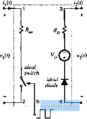 CCM2 Fig. B.3 Subcircuit implementation of the CCM averaged switch model that indudes conduction losses: (a) circuit symbol; (b) PSpice neilis] for the .subcircuil. * MODEL: CCM2 * Applffiation: two-switcdi PWM (inverters, includes * ccnduction [Qses due to Ron. VD, ЯО * Uimitatioris: CCM only, no transformer Parameters: Ron = iransistor on-resistance VOsdiodeferwandvoltagedrop HD = diode on-reslstanoe Nodes: * 1: transistor positive (drain for an n-channel MOS) * 2: transistor negative (source for an n-channel MOS) * 3: diode cathode 4: diode anode * S: duty cycle control input ,subokt семг 1 2 3 4 5 +рагап1з: Ron=0 VD=0 RD=0 Er 1 lx value=(i(Et)(Ron+(l-v(S))RDM5))M5)) Et 1x 2 value=({1-v(5)){v(3.4)+VO)/V(S)} Gd 4 3 valuв={(1-v(5))*i(El)(5)} .ends (Б.4) A subcircuit implementation ofthe averaged switch model described by Eqs. (B.3) and (.B.4) is shown in Fig. B,3 The subcircuit terminal nodes are the same as in the CCMI subcircuit: the transistor port is between the nodes I and 2; the diode port is between the nodes 3 and 4; the duty ratio d ~ i(5) is the con- 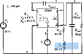 Fig, B,4 StiPIC simulation example. SEPIC DC eonrsion ratio and efficiency Define paranwlars: .param Ron=0.0 VD=0,8 RD=0.05 Analysis setup: .dclinVcO.1 1 0.01 .step lin RARAM Ron 0 1 0.5 Converter netlist: VglOSOV L1 1 2)c 800u RL1 2x2 0.5 10 3x tOOuH RL2 3x 3 0.1 CI ЙЭ lOOuF C2 4 0 lOOuF Xswitch2 04 35CCWI2 tpaiams: Ron=[Ron) VtJ={VD) RD={flD) Rioad4 0 50 Duty cycle input: Vc 5 0 0.5 .lib switch.lib probe .end trol input to the subcircuit at the node 5. Two contrtdled voltage sources in series, E. andffp aie used to generate the port 1 (transistor) averaged voltage according to Eq. (b.3). The controlled voltage source£ models the voltage drop across the equivalent resistance R,Jd(t) + ii{l)Rf/tl(t} iii Eq. (b.3). Note that this equivalent resistance is a nonlinear function of the switch duty cycle d((). The controlled voltage source shows how the port I (transistor) averaged voltage depends on the port 2 (diode) averaged voitage. The controlled current source G models the averaged diode current according to Eq. (b.4). The Subcircuit CCM2 has three pataraetefs (Л , V ;md Л) that can be specified when the subcircuit is used in a converter circuit. The default values of the subcircuit parameters, R = 0, Vp = 0, and Rp - 0, are defined in the .subckt line. These values correspond to the ideal са.че of no conduction losses. The subcircuit CCM2 is included in the model library swilch.Ub. The model of Fig. b.3 is based tm the simple device models of Fig. b.2. It is assumed that inductor current tipples are small and that the converter operates in continuous conduction mode. Many practical converters, however, must operate ni discontinuous conduction mode at low duty сус1е.ч where the diode forward voltage drtip is comparable to or larger than the outpui voltage. In such cases, the model of Fig. b.2, which includes Vq as a fixed voltage generator, gives incorrect, physically impossible results for polarities of converter voltages and currents, losses and efficiency. B.1.3 Example: SEPIC DC Conversion Ratio and Efficiency Let us consider an example of htiw the subcircuit CCM2 can be used lo generate dc conversion ratio and efficieticy curves for a CCM converter. As an example. Figure b.4 shows a SEPIC averaged circuit model. The converter circuit can be foutid in Fig. 6.38(a), or in Fig. 7.37. Toconstruct the averaged circuit model for simulation, the switch network is replaced by the subcircuit CCM2. In the converter netlist shown in Fig. b.4, the .ц-!, line shows how the .subcircuit is connected to other parts of the converter. The switch duty cycle is, set by the voltage source V.. All tit her part.ч of the converter circuit are simply copied to the averaged circuit inodel. Inductor winding resistances /fj = 0.5 £i and - 0.1 П are V/V. 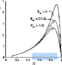 100% 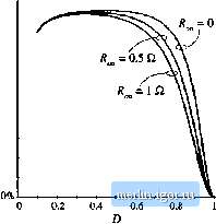 Fig. a.5 SEPIC siittulatiort example: (a) de conversion ratio and (b) efficiency, included to model copper losses of the inductors L and respectively. The switch conduction loss parameters are defined by the .parain line in the netlist: /f, , =0, = 0.8 V, = 0,05 Q. Notice how these values are passed to the subcircuit CCM2 in the X-f line. In this exatnple, all other losses in the cnnverter are neglected. A dc sweep analysis (see the .dc line in the netlist) is set to vary the dc voltage source V. from 0.1 V to 1 V, in 0.01 V increments, which corresponds to varying the switch duty cycle over the range from D = 0.1 to D = 1. The range of duty cycles from zero to 0.1 is not covered because of the model discontinuity probletn at Z) = 0 (discussed in Section B.1.1), and because the model predictions for conduction losses at low duty cycles are not valid, as discussed in Section B.l.2. The dc sweep analysis is repeated for values of the switch on-resistance in the range from R = 0 Й to ff, j = 1 in 0.5 Q. increments (see the .step line in the netlist). The .lib line refers to the swirch.lih library, which contains definitions ofthe subcircuit CCM2 and all other subcircuit models described in this appendix. Simulation results for the dc output voltage Vand the converterefficiency т are shown in Fig. B.5. Several observations can be made based on the modeling approach and discussions presented in Chapter 3. At low duty cycles, efficiency drops because the diode forward voltage dn)p is comparable to the outptit voltage. At higher duty cycles, the converter currents increase, so that the conduction losses increase. Eventually, for duty cycles approaching 1, both the output voltage and the efficiency approach zero. Given a desired dc output voltage and efficiency, the plots in Fig. B.5 can be used to select the transistor with an appropriate value of the on-resistance. B.1.4 Examplt;: Trnsitsnt R !ipon!ie of ti Buck-Booiit Converter In addition to steady-state conversion characteristics, it is often nf interest tn investigate cnnverter transient responses. For exaraple, in voltage regulator designs, it is necessary to verify whether the otitput voltage remains within specified limits when the load current talces a step change. As another example, during a start-up transient when the converter is powered up, cnnverter comptments can be exposed to significantly higher stresses than in steady state. It is of interest to verify that component stresses are |