
|
| |
|
Строительный блокнот Introduction to electronics Rg, B.6 Butk-boost converter example. Switch necwoiH l5riH 50jlF within specifications or to niaketlesign mollifications to retiuce the stresses. In these examples, transient simulations can 1зе used to test for converter responses. Transient simulations can 1зе performed on the converter switching circuit model or on the converter averaged circuit model. As an example, let us apply these two approaches to investigate a start-up transient response of the buck-b )st converter shown in Fig. B.6. Figure B.7 shows a switching circuit mtxlel of the buck-boost converter. The inductor winding resistance R is included to mtxlel the inductor copper losses. The MOSFET is modeled as a voltage-controlled switch controlled by a pulsating voltage source v.. The switch .mtxlel line specifies the switch on-reststance = 50 mil, and the switch off-resistance R = 10 M£2. The switch is on when the controlling voltage is greater than V, = 6 V, and off when the controlling voltage v. is less than V = 4V. The pulsating source has the pulse amplitude equal to 10 V. The period is T. = Uf = 10 fls, the rise and fall times are = tf = 100 ns, and the pulse width is t = 7.9 s. The switch duty cycle is D = (fp + 0.5((+ tj))/Tj.-(i.&. The built-in nonlinear Spice model is used for the diode. In the diode .model statement, only the parameteris specified, to set the forward voltage drop across the diode. The switch and the diode models used in this example are very simple. Conduction losses are modeled in a simple manner, and details of complex device behavior during switching transitions are neglected. 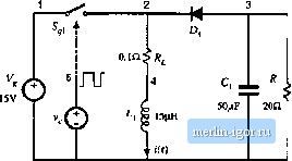 v(t) Buek-tjoost cottve/ter; awftctiing clnxilt Vg 1 015V Sql 1 ZSOswtlrti Dt 3 2 diode RL2 4 0,1 Ll 4 015uH ic=0 CI 3 0 50tjFic=0 R 3020 Vc 5 0 pulse +(0 10V Ous 100ГВ tOOrs 7,Эив lOus) .model swrtofi vsvntoh +(Ron=o,05 Roft=10ir>eg Von=6V Voff=4V) .model diode d(ls=19-12) tran 1u 1.2m Om Iu uk: probe .end Fig, B,7 Buck-boost converter simulation example, switching circuit model. CCM2 я 0.05 a V = 0.8V 0.inSRj. SOjiF Buiic-boost converter, averaged circuit .lib svinlch.№ VglOISV Xsviritch 1 2 2 3 5 CCM2 + FWRAMS: Bon=0.05 VD=0,8 R0=0 RL2 4 0.1 L14 016UH tc=0 C13 0 50uFic=0 nsoso Vc5 00.e .Iran lOu 1.2m Om lOu uic .prtAe .ei4l Fig. B.8 Buck-boost cortverter simulation example, averaged circuit model. Therefore, the circuit mtxiel of Fig. B.7 ctinnot be used to examitie switching transitions or to predict switching los.ses in the convetter. Neverthele.4.4, ba.sic switching operation is modeled, and a transient simulatioti c;m be u.4ed to fmd out how the converter wavefonns evolve iti time over many switching cycles. Tratisient sitnulation parameters жи defined by the .tran line: the output time step is 1 (is, the final simulation time is 1.2 tns, the output wavefortns iu-e genettited from the statt of simulation at time equal to zero, iind the tnaxitnutn tillowed time step is 1 14S. The uic ( use initial conditions ) option tells the simulator to .start with all capacitor voltages and inductor currents etjuiil to the specified initial values. For example, ic=(> in the tj line sets the initial inductorcurrent to zero. In Spice, the default initial conditions are always zero, so that ic=0 statements can be omitted. An averaged circuit model of tiie buck-boost converter is .siiowii in Fig. B.8. This circuit mtxiel is obtained by replacing tiie .switch network in the cotiverter of Fig. B.ft by the CCM2 subcircuit. Notice that the circuits and the netlists of Figs. B.7 and Fig. B.S iu-e vety similar. The tmly difference is that the switchitig devices in the cotiverter circuit of Fig. B.7 iire replaced by the CCIVI2 subcircuit Х,н;, in Fig. B.8. Also, the pulsating source v(f) in the switching circuit is replaced by a cotistant voltage .source Vj, equal to the switch duty cycle D = 0.8. The inductor current and the capacitor voitiige waveforms duritig the start-up transient iue shown in Fig. B.9. For compiirisoti, the waveforms obtained by transient simulatioti of tiie switciiiiig convertercircuit shown in Fig. B.7, and by simulation ofthe iiveniged circuit model ofFig. B.8 iue shown. Switching ripples ciin be observed in the wiivefoims obtained by simulation of tiie switching circuit mtxiel. The converter transient response is governed by the cotiverter natural time constants. Since these time constants are much longer than the switching petitxl, the converter stiut-up transient responses in Fig. B.9 take many switching cycles to reiich the steady state, hi the results obtained by simulation of tiie averaged circuit model, tiie switching ripples are removed, but the low-frequency portions of the converter transient responses, which are governed by the natural time constants of the converter network, match very clo.sely the responses obtained by simulation ofthe switching circuit. Based on the results shown in Fig. B.9, we ciin see that converter components iu-e expo.sed to significantly higher current stresses during the stiitt-up transient than during steady state opetiition. The probletn of excessive stresses in the start-up transient is quite typical for switching power convetters. Practical designs usuiilly include a soft-start circuit, where the switch duty cycle i.s slowly incTetrsed Waveform obiained by simulation of the averaged model , Waveform obtained by simulation of the switching circuii model 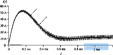 1.2 ms 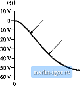 Waveform obtained by simulation of the averaged model Waveform obtained by simulation of the switching circuit model !-1- 0.2 ms 0.4 ms 0.6 ms O.a ms 1 ms 1.2 ms Fig. b.9 Inductor current and output voltage wavefonns obtaitied by transient sitnulation of the switching converter circuit shown in Fig B.7, and by simulation of the averaged circuit model of Fig. b.8 from zero to the steady-slate value to reduce start-up transient stresses. This simulation example illostrates how an averaged circuit model can be used in place of a switching circuit tnodel to investigate converter large-signal transient responses. An advantage of the averaged circuit tnodel is that transient simulations can be cotnpleted mtich tnore quickly because the averaged mtxlel is time invariant, and the siinulntor does not spend time computing the details of the fast switching transitions. This advantage can be important in sitnnlations of larger electronic systetns that include switching powerconverters. Another itnportant advantage also comes frotn the fact that the averaged circuit model is nonlinear but time-invariant: ac simulations can be used to linearize the mtxlel and generate small-signal freqtiency responses of interest. This is not possible with switching circuit models. Examples of small-signal ac simulations can be found in Sections B,2 and B.3. combined ссмдасм avera(;ed switch model The models and exatnples of Section B.l are all ba.sed on the assumption that the converters operate in continuous conduction mode (CCM). As discussed in Chapters 5 and 11, all converters containing a diode rectifier operate in discontinuous conduction mode (DCM) if the load cuitent is sufficiently low. In some cases, converters are purposely designed to operate in DCM. It is therefore of interest to develop |