
|
| |
|
Строительный блокнот Introduction to electronics points, the quiescent (de) voltiiges and currents in the ciicuit iire nearly the same. Nevertheless, the frequency responses tire qualitatively very different in the two operating tnodes. In CCM, the converter exhibits a fourth-order re.4pot1.4e with two pairs of high-2 complex-conjugate poles and a pair of complex-conjugate zeros. Another RHP (right-half plane) zero can be observed at frequencies approaching 50 kHz. In DCM, there is adominaut low-frequency pole followed by a pairof complex-conjugate poles and a pair of complex-conjugate zeros. The frequencies of the complex poles and zeros are very close in value. A high-frequency pole and a RHP zero conttibute additional phase lag at higher frequeitcies. In the design ofa feedback controller around a converter that may operate in CCM or in DCM, one should take into account that the crossover frequency, the phase margin, and the closed-loop respoiLses ctm be substantially different depending on the operating tnode. This point is illustrated by the exatnple of the next section. 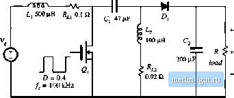 120 V 120 V L,500pH 0.1a SEPIC frequency response ... Other parts ot the netlist omitted ... duty cycle inpul: vc 5 Ode 0.4 ac 1 subcircuit Xswitdt 2 04 3 5 CCM-DCMl + PARAMSj L=e3.3uH !в=100кНг ,11b switch.lib anysis setup: ,ac dec 201 5 50kHz .end Ci 47 (iF ССМ-СЮМ1 200 HF = load switch /.= S3.3iH /,= 11ЮкНг Fig, B.13 SEPIC simulation example; (a) converter circuit, (b) averaged circuit model for simulation. 80 dBV 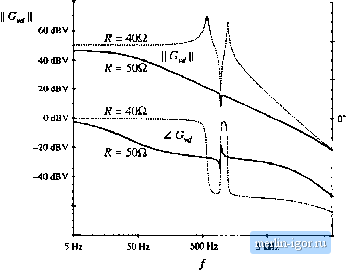 .-90* -180 -270* 50 Шг Fig. B.14 Magnitude and phase responses of the control-to-output transfer function obtained by simulation of the SEPIC example, lor two vahiea of tbe load resistance. For Л = 50 Й, the converter operates in DCM (solid lines), and for Д = 40 SI, the converter operates in CCM (dotted lines). B.2.2 Example: Loop Uain and Closed-Loop Responses of a Buck Voltage Regulator A controller design for a buclt converter example is discussed in Section 9.5.4. The converter and the block diagram ofthe controller are shown in Fig. 9.22. This converter system is designed to regulate the dc output voltage at V= 15 V for the load current up to 5 A. Let us test this design by simulation. An averaged circuit model of a practical realization of the buck voltage regulator described in Section 9.5.4 is shown in Fig, B,15. The MOSFET and the diode switch are replaced by the averaged switch model implemented as the CCM-DCMl subcircuit. The pulse-width modulator with = 4 V is modeled according to the discus.sion in Section 7.fi as a dependent voltage source E controlled by the PWM input voltage v. The value of fij , is equal to ifVj = 0.25 times the PWM input voltage v, with a limit for the minimum value set to 0.1 V, and a limit for the maximum value set to 0.9 V. The outptit of the pulse-width modulator is the control duty-cycle input to the CCM-DCMl averaged switch subcircuit. Given the specified limits for £ , , the switch duty cycle d{tj can take values in the range: fJ , <rf(l)<0. (D.S) where = 0.1, and D = 0.9. Practical PWM integrated circuits often have a limit D , < 1 for the maximum possible duty cycle. The voltage sensor and the compensator tire implemented around an op-amp LM324. With very large loop gain in the system, the steady-state error voltage is approximately zero, i.e., the dc voltages at the plus and the tniiius inputs of the op-amp are almost the same. v(5)= V (B.9) As a result, the quiescent (dc) oittput voltage V is set by the reference voltage vjand the voltage divider comprised of R, /2 4- (B.IO) By setting the ac reference voltage f,;,;-to zero, the combined transfer function of the voltage setisor atid the compensator can be fotmd as: This transfer function can be written in factored pole-zero form as where G,.ff (B.ll) © 4=100 kHz L SOpH 3 U>AD * It kfl * S5kn 120 kn +12 V value = {LIMim26 v, CI, C9)J © .nodesat v(3).15 v(5)rf v(6)=:4.t44 v(e)=D.S36 1.1 nF 47 Ш Fig. B.15 Buck voltage regulator example. |