
|
| |
|
Строительный блокнот Introduction to electronics G., N = 1 (B.13} fi, + k; 271 2ЯД2С3 {B.141 The design described in Section У.5.4 resulted in the following values for the gain and the comer frequencies: С ,Я=3.7(1/3) = 1,23, /,= 1.7kHz, Д = 500Нг, 14,5kHz (ВП) Eqs. (B.IO) and (B.13) to (B.17) can be used to select the circuit parameter values. Let its (somewhat arbitrarily) choose = 1,1 nF. Then, from Eq. (B.14), we have R- Il Eq. (B.16) yields Д = 11Ш. From Eq. (B.13) we obtain ffj = 120 кП, and Eq. (B. 15) gives C\ - 2.7 кй. Finally, Л = 47Ш is found from Eq. (B.IO). The voltage regulator design can now be tested by simulations of the circuit in Fig. B.l5. Uwp gains can be obtained by simulation using exactly the same techniques described in Section 9.6 for experimental measurement of loop gains [20]. Let us apply the voltage injection technique of Section 9.6.1. An ac voltage source is injected between the compensator otitput and the PWM input. This is a good injection point since the output impedance ofthe compensator built around the op-amp is small, and the PWM tnput impedance is very large (infinity in the circuit model of Fig. B.15). With the ac source amplitude set (arbitrarily) to 1, and no other ac sources in the circuit, ac simulations are performed to find the Itxip gain as v 47) To perform ac analysis, the simulator first solves for the quiescent (dc) operating point. The circuit is then linearized at this operating point, and small-signal frequency responses are computed for the specified range of signal frequencies. Solving for the quiescent operating point involves numerical solution of a system of nonlinear equations. In some cases, the numerical solution does notconverge and the simulation is aborted with an error message. In particular, convergence problems often occur in circuits with feedback, especially when the loop gain atdc is very large. This is the case in the circuit of Fig. B.15. To help convergence when the simulator is solving for the quiescent operating point, one can specify approximate or expected values of node voltages using the .mxieset line as shown in Fig. B.15. In this case, we know by design that the quiescent output voltage is close to 15 V (i(3) = 15), that the negative input of the op-amp is very close to the reference (i(5) = 5), and that the quiescent duty cycle is approximately D = WVj =0.536, so that v(S) - 0.536 V. Given these approximate node voltages, the numerical solution converges, and the following quiescent operating points are found by the simulator for two values of the load resistance R: 60 dB Fig. Ii.l6 1лор gain in the baclc voltage legiilator exaaiple. = 5.3 kHz 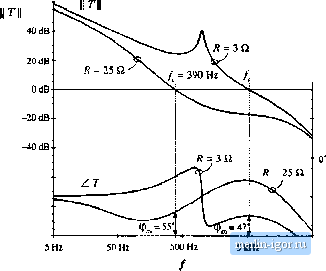 -180 SO kHz fi = 3 U, v(3) = 15.2 V, t<.J> = S,0 V, v(7> = 2. i73 V, r(8) = 0,S43 V, fJ = О-.НЗ (В.1У) я = 2S a. v(3)= 15.2 V, v(5) = 5Л) V, i(7) = 2,033 V. US) = 0.Ш V, /: = fi.SOB (□.20) For the nominal load distance A = 3 П, the conveiter opeiate.4 m CCM, .чо that D = VfV. For Л = 25 Й, the same dc output voltage is obtained for a lower value of the quiescent duty cycle, whtch means that the converter operates in DCM. The magnittide and phase responses of the loop gain found for the operating points given by Eqs. (B.19) and {B.2()) are shown in Fig. B.16. For A 3 tl, the crossover ftequency is,/j =5,3 kHz, and the phase margin is ф = 47°, very close to the values (f-5 kHz, i/f = 52°) that we designed for in Section 9.5.4. At light load, for Л = 25 Q, the loop gain responses are con.siderably different becau.se the converter operates in DCM. The crossover frequency drops to f = ЗУО Hz, while the phase margin is Фм = 55°. The magnitude respon.ses of the line-to-output transfer function are shown in Fig. B.17, again for two values of the load resistance, Л = 3 il and R = 25 Q. The open-loop responses are obtained by braking the feedback loop at node S, and setting the dc voltage at this node to the quiescent value D of the duty cycle. For R-3Q, the open-loop and closed-loop responses can be compared to the theoretical plots shown in Fig. 9.32. At 1(K) Hz, the closed-loop magnitude response is 0.012 =>-38 dB, .A 1 V, KM) Hz variation in v,{r) would induce a 12 mV variation in the output voltage vff). For R-25 il, the closed loop magnitude response is 0.02 => - 34 dB, which means that the 1 V, 100 Hz variation in v(f) would induce a 20 inV variation in the output voltage. Notice how the regulator performance in terms of rejecting the input voltage disturbance is significantly worse at light load than at the nominal load. A test of the transient response to a step change in load is shown in Fig. B.18. The load ctirrent is initially equal to 1.5 A, and increases to fxiAp - at r = 0.1 tns. When the converter is operated in B.2 CDmbined CCM/DCM Averaged Switch Mode! 70 JB Fig, B.17 Line to output response ol tlie bttck voltage regulator. fi = 3Q 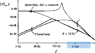 JOkHz 16 V- ISV- 14 V 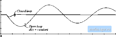 6A 4 A 0.2 ms 0.4 ms 0.6 ms 0.£nis 1.0 ms t.2iiiis 1.4 ms 1.6 ms 1.8 ms ms 0 0.2 ms 0.4 ms 0.6 0-4rns t.Oms 1.2mi 1.4ms t.ums 1.8 ni$ 2.0 t Fig, B.18 Load transient response of the buck voltage regalator example. open loop at constant duty cycle, the response is governed by the natural time constants of the converter network, A large undershoot and long lightly-damped oscillations can be observed in the output voltage. With the feedback loop closed, the controller dynamically adjusts the duty cycle d{r) trjing to maintain the output voltage constant. The t)Utput voltage drops by about 0.2 V, and it returns to the regulated value after a short, well-damped transient. The voltage regulator example ofFig. B.15 illustrates how the performance can vary significantly if the regulator is expected to supply a wide range of loads. In practice, further tests would also be performed to account for expected ranges of input vohages, and variations in component parameter values. Design iterations may be necessary to ensure that performance specifications are met under worst case conditions. |