
|
| |
|
Строительный блокнот Introduction to electronics Base Emitter A , 1771 , Г /777П , 1771 , Г J. J L Fig. 4.30 Power BJT struclurc. Ciosshiitolled regions are metallized cotHacts. /. 777T7/y /?77 ЛЛг CoUector resistance via the condnctivity modulation effect. Between the off state and the on state is the familiar active region, in whicli tlie/wi base-emitterjtinction is forward-biased and the p-fl base-collector junction is reversc-biiiscd. When the BJT operates in the active region, the collector current is proportional to the base region minority charge, which in turn is proportional (in equilibrium) to the base current. There is in addition a fourth region of operation known as cjuasi-saturanon, occurring between the active and saturation regions. Quasi-saturation occtirs when the base current is instifficient to fully saturate the device; hence, the minority charge present in the n~ region is insufficient to fully reduce the n~ region resistance, and high transistor on-resistance is observed. Consider the simple switching circuit of Fig. 4.31. Figure 4.32 contains waveforms illustrating the BJT turn-on and turn-off transitions. The transistor operates in the off state during interval (1), with the base-emitterjtinction reverse-biased by the source vohage v,(f) = - V,.. The turn-on transition is initiated at the beginning of interval (2), when the .source voltage changes to vp) - + Positive current is then supplied by source to the ba.se of the BJT. This current first charges the capacitances of the depletion regions of the reverse-biased base-emitter and base-collector junctions. At the end of interval (2), the ba.se-emitter voltage exceeds zero sufficiently for the base-emitter junction to become forward-biased. The length of interval (2) is called the turn-on delay time. During interval (3K minority chiirge is injected across the base-emitter jrmction from the emitter into the base region; the collector current is proportional to this minority base charge. Hence during interval (3), the collector current increases. Since the transistor drives a resistive load the collector voltage also decreases during interval (3). This causes the voltage to reduce across the reverse-biased base-collector depletion region (Miller) capacitance. Increasing the b;Lse current /д, (by reducing R or increasing Vj) increases the rate of change of both the base region minority charge and the charge in the Miller capacitance, Hence, increased leads to a decrea.sed turti-oti switching time. Near or at the end of interval (3), the base-collector р-н junction becomes forward-biased. Minority carriers are then injected into the n region, reducing its effective resistivity. Depending on the device geometry and the magnitude of the base ctirrent, a voltage tail [interval (4)] may be observed as Fig. 4.31 Circuit for BJT switching time example. 0.7 V 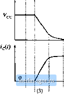 -9rr (1) <2) <4) i (3) = (6) i (7) m Fig. 4.32 BJT turn-oil and tutn-off transition waveforms. tlie apparent resistance of the/l~ region decreases via conductivity modulation. The BJT reaches on-state equilibrium at the beginning of interval (5), with low on-resistance and with substantial minority charge present in both the n~ andp regions. This minority charge significantly exceeds the mnount neces.saiy to support the active region conduction of the collector current /f,,; its magnitude is a function of /д[ - l(j,J?>, where p is the active-region current gain. The tnrn-off process is initiated at the beginning of interval (6), when the source voltage changes to vjil) = - V,. The base-emitter junction remains forward-biased as long as iinority carriers are present in its vicinity. Also, the collector current continues to be if~(t) = / as long as the minority Swdch Realization Fig, 4.33 Ideal base current waveform for fninimi-zation of switctiing times. it charge exceeds the amount necessary to support the active region conduction ofthat is, as long as excess charge is present. So during interval (6), a negative base current flows equal to -/jj = (- Vjj - VijJ,t))IRif. This negative base current actively removes the total stored minority charge. Recombination further reduces the stored minority charge. Interval (6) ends when all of the excess minority charge has been removed. The length of interval (Й) is called the storage time. During interval (7), the transistor operates in the active region. The collector current i(t) is now proportional to the stored minority charge. Recombination and the negative base current continue to reduce the minority base charge, and hence the collector decreases. In addition, the collector voltage increases, and hence the base current must charge the Miller capacitance. At the end of interval (7), the minority stored charge is equal to zero, and the base-emitter junction can become reverse-biased. The length of interval (7) is called the turn-off time or fall time. During interval (8), the reverse-biased base-emitter junction capacitance is discharged to voltage - V,;. During interval (9), the transistor operates in equilibrium, in the off state. It is possible to turn the transistor off using /j = 0; for example, we could let V.j be approximately zero. However, this leads to very long storage and turn-off switching times. If I = then all of the stored minority charge must be removed passively, via recombination. From the standpoint of minimizing switching times, the base current waveform of Fig, 4.33 is ideal. The initial base current / is large in magnitude, such that charge is inserted quickly into the base, and the turn-on switching times are .short. A compromise value of equilibrium on state current /, is chosen, to yield a reasonably low col-lector-to-eraitter forward voltage drop, while maintaining moderate amounts of excess stored minority charge and hence keeping the storage time reasonably short. The current - /j is large in magnitude, such that charge is removed quickly from the base and hence the storage and turn-off switching times are minimized. Unfortunately, in most BJTs, the magnitudes of /ц[ and /g; must be limited because excessive values lead to device failure. As illustrated in Fig. 4.34, the base current flows laterally through the p Base 9 Ettiitter rZTTI tzzzz ZZZZL JZZZL Fig. 4.34 A large / leads to focusing of the emitter current nwuy from the base contacts, due to the voltage indiiocd by the lateral base region current. 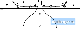 |