
|
| |
|
Строительный блокнот Introduction to electronics ТППГ
1 : л Fig, CilS Measurement of Z(s) and Z (j): (a) determination of Z;j(i), (b) determination otZs). Under the conditions that the transformer is ideal (i.e., the transformer magnetizinj open eiretiited), then the transfer ftmction is given by: C(.(), inductance L/ is (C.36) We ean therefore employ the extra element theorem to determine how finite magnetizing inductance changes G(s). With reference to Fig. C. I, the system input is v (.?), the output is the voltage vj), and the port is the primary winding of the transformer, where the magnetizing inductance is connected. In the presence of the magnetizing inductance, the transfer ftmction becomes G(i) = Z(j) j (C.37) where S,s) is the impedance of the magnetizing inductance referred to the primary winding, sLi. Figure C.15(a) illustrates determination ofZQ(j). The input source Vj(i) is set to zero, and the impedance between the terminals of the port is fotmd. It can be seen that the impedance ZQ(f) is the parallel combination of the impedances of the tank indtictor, tank capacitor, and the reflected load resi-tance: (C.3S) Figure C.15(b) illustrates determination of Zy(.r). In the presence of the input .source Vj[(.r), a Current i(.r) is injected at the port as shown. This current is adjusted such that the output vj[s) is nulled. Under these conditions, the quantity Zj) is given by v(s)li(.\}. It can be seen that nulling v {s) also nulls the voltage vis). Therefore, 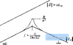 Fig. СЛ6 To avoid signifitantly changing the transfer function G(s). the transfoftner should be designed such that Z . 7 u\- {C.39) Note that, in general, i(s) will not be equal to zero during the Zf{s) measurement. The null condition is achieved by setting the source equal to the value - V(j!)JsL. Thus, in the presence of finite magnetizing inductance, the transfer function G(s) can be expressed as follows: ic.m We can now plot the impedance inequalities (C.27) that guarantee that the magnetizing inductance does not stibstantially modify C(.c). The Zp{s) given in Eq. (C.38) is the impedance of a parallel re.sonant circuit. Con.4truction of the magnitude of this impedance is described iu Section 8.3.4, with results illustrated in Fig. C.16. To avoid affecting the transfer function C(j), the impedance ofthe magnetizing inductance must be much greater than Zjijisi) over the range of expected operating frequencies. It can be seen that this will indeed be the case provided that the impedance of the magnetizing inductance is greater than the impedances of both the tank inductance and the reflected load impedance: L 3i. L, and where 0)0= \/{JlC) . These conditions can be further reduced to Lu~ - E, and (C.41) (C,42) C.4.3 Addition uf an Input Filter tu a Cunverter As discussed in Chapter 10, the addition of an input filter to a switching regulator can significantly alter its loop gain T{s). Hence, it is desirable to design the input filter so that it does not substantially change © Input filter Converler
ns)] Fig. C,17 Addition of an input filter to a switching voltage regulator system. tlie converter eontroi-to-output transferfunction GjW. The Extra Element Theorem can provide design criteria that show how to design such an input filter. Figtire C.17 illustrates the addition of an input filter to a switching voltage regulator system. The control-to-output transfer function of the converter power stage is given by: GJs) v{s) J(s) (CAi) ; t>)= The quantity Zfs) is the Thevenin equivalent output impedance of the input filter. Upon setting v{s) to zero in Fig. C.17, the system of Fig. CIS is obtained. It can be recognized that this system is of the same form as Fig. C.2, in which the extra element is the output impedance ZJs) of the added input filter. With no input filter \ZJjs) = 0], the original transfer function Gi,/OI,f,) is obtained. In the presence of the input filter, C!,j(s) is expressed according to Eq. (C.3): Z(s) \ Z,v(.v) Z(s) -Z {s) fC.44) where Z (.v)= Z,(i} (C.45} Fig, CIS Determination of tho control-to-ouiput transfer J.) fmicdoii Gj.jf.O for die system of Fig, C,17. Converter GJs)/ |
||||||||||||||||