
|
| |
|
Строительный блокнот Introduction to electronics Fig. 4.43 Negative gate curient is iinabie tii cotnpletely reverse-bias Ihe gaie-cathude junetion, Tlie anode current focuses away from the gate co!itact. ZZZZZZZZZZZL.JZ22ZZL ZZZl 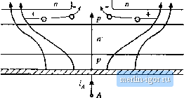 The turn-off gain of a GTO is the ratio of on-state current to the negative gate current magnitude required to switch the device off. Typical values of this gain are 2 to 5, meaning that several hundred imiperes of negative gate current may be required to turn off a GTO conducting 1000 A. Also of interest i.4 the maximum controllable on-state current. The GTO is able to conduct peak currents .significantly greater than the rated average current; however, it may itot be possible to switch the device off under gate control while these high peak currents are present. The MOS-controiied thyristor, or MCT, is a recent power device in which MOSFETs are integrated onto a highly interdigitated SCR, to control the turn-on and turn-off proces.ses. Like the MOSFET and IGBT the MCT i.s a single-quadrant device whose turn-on and turn-off transitions are controlled by a MOS gate terminal. Commercial MCTs srnp-typc devices. Voltage-bidirectional two-quadrant MCTs, and H-type MCTs, are also possible. A cross-section of an МСЛ containing MOSFETs for control tif the turn-on and turn-off transitions is illustrated in Fig. 4.44. An equivalent circuit which explains the operation of this structure is given in Fig. 4.45. To turn the device on, the gate-to-anode voltage is driven negative. This forward-biases p-channel MOSFET Q, forward-biasing the base-emitterjunction of BJT Qy Transistors and Q2 then latch in the on-state. Tti turn the device off, the gate-to-anode voltage is driven positive. This forward-biases и-chiinnel MOSFET Q, which in turn reverse-biases the base-emitterjunction of BJT Qj. Tlie BJTs then turn off. It is important that the on-resistance of the и-channel MOSFET be small enough p Anode Care Fifi, 4.44 MCT structure, Crosshatcltcd regions arc metallised contacts. Lightly shaded regions are insulating silicoti dioxide luvers. 2j channel channel Cathode 0 Cathode Ilg. 4.4s Ecitivi letW circuit tor the MCT, Gate Anode that sufficient influence on the cathode current is exerted-this limit.s tlte maximum coittroilabk oit state current (i.e., the maximum current that can be interrupted via gate control). High-voltage MCTs exhibit lower forward voltage drops and higher current densities than IGBTs of similar voitage ratings and siiicou area. However, the switching times are longer. Like the GTO, the MCT can conduct considerable surge currents; but again, the maximum current that can be interrupted via gate control is limited. To obtain a reliable turn-off transition, external sniibbeis are required to limit the peak anode-to-cathode voltage. .A sufficiently fast gate-vohage rise time is also required. To some extent, the MCT is still an emerging device-future generations of MCTs may exhibit considerable improvements in performance and ratings. SWn CHIN (; LOSS Having implemented the switches using semiconductor devices, we can now discuss another toajor source of loss and inefficiency in converters: switching loss. As discussed in the previous section, the turn-on and turit-off transitioits of semiconductor devices require times of tens of itanosecouds to microseconds. During these switching transitions, very large instantaneous power loss can occur in the semiconductor devices. Even though the seiniconductor switching times are short, the resulting average power loss can be significant. Semiconductor devices are charge controlled. For example, the conducting state of a MOSFET is determined by the charge on its gate and in its channel, and the conducting state of a silicon diode or a BJT is determined by the presence or absence of stored minority charge in the vicinity of the semiconductor junctions inside the device. To switch a semiconductor device between the on and off states, the controlling charge must be inserted or removed; hence, the amount of controlling charge influences both the switching times and the switching k)ss. Charge, and energy, are also stored in the output capacitances of semiconductor devices, aitd energy is stored in the leakage and stray inductances iit the circuit. In most converter circuits, these stored energies are also lost during the switching transitions. In this section the major sources of switching loss are described, and a simple method for estimation of their magnitudes is given. For clarity, conduction los.ses and seiniconductor forward voltage drops are neglected throughout this discussion. Physical i,U) I MOSFET T Ф . ЧУ - 7\ driver Fig. 4.46 MO.SHET driving a clamped inductive load, liuck converter example, 4.3.1 Transistor Switching with Clamped inductive Load Lets consider first the switching waveforms in the buck converter of Fig. 4.4Й. Let us treat the diode as ideal, and investigate only the switching loss due to the MOSFET switching times. The MOSFET drain-to-source capacitance is also neglected. The diode and inductor present a clamped inductive load to the transistor, With such a load, the transistor voltage f(f) and current fCOdo not change simnltaneously. Forexample, a magnified view of the transistor turn-off-transition waveforms is given in Fig. 4.47. For simplicity, the waveform.4 ше Transistor wavefurms Fig. 4.47 Magnihed view of transistor turn-off transition waveforms for the circuit of Fig, 4.4Й. 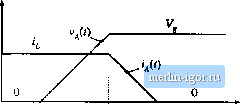 Diode waveforms 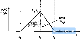 |