
|
| |
|
Строительный блокнот Introduction to electronics 94 Switch ReaiimioK approximated as piecewise-iinear, The switching times are short, such that the indtictor current 1,(0 is essentially constant during the entire switching transition i<t < (j. No current flows through the diode while the diode is reverse-biased, and the diode cannot become forward-biased while its voltage Vg(;) is negative. So first, the voltage across the transistor must rise from zero to V. The interval length Oj-Zfj) is essentially the time required for the gate driver to charge the MOSFET gate-to-drain capacitance. The transistor current is constant and equal to t during this interval, The diode voltage vit) and current are given by v,{i)=v,{t)-V i (0 + iU) = At time i= (j, when = V, the diode becomes forward-biased. The current now begins to commute from the transistor to the diode. The interval length (f2~i5 time required for the gate driver to discharge the MOSFET gate-to-souice capacitance down to the threshold voltage which causes the MOSFET to be in the off state. The instantaneous power p{t) dissipated by the transistor is equal to 1д(0д() This quantity is also sketched in Fig. 4.47. The energy VV j lost during the transistor turn-off transition is the area under this waveform. With the simplifying assumption that the waveforms are piecewise-iinear, then the energy lost is the area of the shaded triangle: This is the energy lost during each transistor turn-off transition in the simplified circtiit of Fig. 4.46. The transistor turn-on waveforms of the simplified circtiit of Fig. 4.46 are qualitatively similar to those of Fig. 4.47, with the time axis reversed. The transistor current must first rise from 0 to г- The diode then becomes reverse-biased, and the transistor voltage can fall from to zero. The instantaneous transistor power dissipation again has peak value VJ, aitd if the waveforms are piecewise linear, then the energy lost during the tuiit-oit transition iV, , is given by {) S V,( multiplied by the transistor turn-on time. Thtis, during one complete switching period, the total energy lost during the turn-on and turn-off transitions is (Wj + ,fj)- If the switching frequency is/ then the average power loss incurred due to switching is ,wii-hing So the switching loss is directly proportional to the switching frequency, Alt example where the loss due to transistor switching times is particularly significant is the current tailing phenomenon observed during the turn-off transition of the IGBT. As discussed iit Section 4.2.4, current tailing occurs due to the slow recombination of stored minority charge in the n region of the IGBT. This causes the collector current to slowly decay after the gate voltage has been removed. A buck converter circuit containing an ideal diode and nonideal (physical) IGBT is illustrated in Fig. 4.48. Ttnit-off transition waveforms are illustrated in Fig. 4.49; these waveforms are similar to the MOSFET waveforms of Fig. 4.47. Tlte diode is initially reverse-biased, and the voltage v{t) ri.ses from approximately zero to V. The interval length (( - Iq) к the time required for the gate drive circuit to charge the IGBT gate-to-collector capacitance. At time t- t, the diode becomes forward-biased, and current begins to commute from the IGBT to the diode. The interval (f -/j) is the time required for the gate drive circuit to discharge tlte IGBT gate-to-eraitter capacitance to the threshold value which causes Physical РГ, driver diode Fig. 4,48 IGBT switching loss; sxample. the effective IVIOSFET in Fig. 4.38(h) to be in the off state. This time can be miniraizeii by use of a high-current gate iJrive circuit which discharges the gate capacitance quicltly. However, switching off the effective IVlOSFET does not completely interrupt the IGBT currem iff,t)- current continues to flow through the effective PNP bipolarjunction transistor of Fig. 4.38(b) as long as minority carriers continue to exist within its base region. During the interval < i < /3, the current is proportional to this stored minority charge, and the current tail interval length ((3 - /2) is equal to the time required for this remaining stored minority charge to recombine. The energy Wjf lost during the turn-off transition of the IGBT is again the area under the instantaneous power waveform, as illustrated in Fig. 4.49. The switching loss can again be evaluated using Eq. (4.S). The switching times of the IGBT are typically in the vicinity of 0.2 to 2 lis, or several times JGBT waveforms Diode ifaveforins Fig, 4,49 IGDT lurn-off transition waveforms for the circuit of Fig, 4.48. 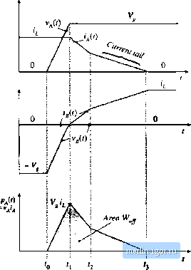 longer tliiin those of the power MOSFET. Tlie resulting switching lo.w limits tiie maximum switching frequencies of conventional PWM converters employing IGBTs to roughly 1 to 30 kHz. 4.3.2 Diode Recovered Charge As discussed previously, the familiar exponential i-v characteristic of the diffused-junction p-n diode is an equilibrium relationship. During switching transients, significant deviations from this characteristic are observed, which can induce transistor switching loss. In particular, during the diode turn-off transient, its stored minority charge must be removed, either actively via negative current or passively via recombination inside tlie device. The diode remains forward-biased while minority charge is present in the vicinity of the diode semiconductorjunction. The initial amount of minority charge is a function of the forward current, and its rate of change, under forward-biased conditions. The turn-off switching time is the time required to remove all of this charge, and to establish a new reverse-biased operating point. This process of switching the diode from the forward-biased to reverse-biased states is called reverse recovery. Again, most diffused-junction power diodes are actually p-n~-n* or p-i-n devices. The lightly doped or intrinsic region (of the diode and other power semiconductor devices us well) allows large breakdown voltages to be obtained. Under steady-state forward-biased conditions, a substantial amount of stored charge is present in this region, increasing its conductivity and leading to a low diode tm-resis-tance. It takes time to insert and remove this charge, however, so there is a tradeoff between high breakdown voltage, low on-resistance, and fast switching times. To understand how the diode stored charge induces transistor switching loss, let us consider the buck converter of Fig. 4.50. Assume for this discussion that the transistor switching times are much faster than the switching times of the diode, such that the diode reverse recovery mechanism is the only significant .чоигсе of switching loss. A magnified view of the transistoi-turn-on transition waveforms under these conditions is given in Fig. 4.51. Initially, the diode conducts the inductor currenl, and hence some amount of stored minority chaige is present in the diode. The transistor is initially in the off state. When the transistor turns on, a negative cuirent flows through the diode; this current actively removes some or most of the diode stored minority charge, while the remainder of the minority charge recorabines within the diode. The rate of change of the current is typically limited by the package inductance and other stray inductances present in the external circuit; hence, the peak magnitude of the reverse current depends on the external circuit, and can be many times larger than the forward current i. The area within the negative portion of the diode current waveform is the recovered stored charge {? while the interval length (f; - Гц) is the reverse recovery time t. The magnitude of is a function of the on state forward current at the initiation of the turn-off process, as well as the circuit-limited rate-of-change of the diode current, dig(i)l(h. During 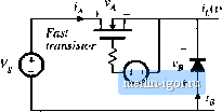 Silicon -> diode I < Fig. 4.59 Example, switching loss induced by diode stoied charge. |